Optical filter and optical device using same

An optical filter and optical device technology, applied in the field of optical filters, can solve the problems of poor out-of-band suppression characteristics, high incidence angle dependence of free spectral range, difficulty in reducing the size of the spectrometer, etc., and achieves the possibility of loss of optical waveguide structure. Minimize variability, monitor and optimize thickness effects in real time

Inactive Publication Date: 2019-04-02
SAMSUNG ELECTRONICS CO LTD
View PDF7 Cites 9 Cited by
  • Summary
  • Abstract
  • Description
  • Claims
  • Application Information

AI Technical Summary

Problems solved by technology

[0003] The advantage of the Fabry-Perot filter using the optical interference effect is that it is relatively easy to control the transmission center wavelength and transmission bandwidth, but the disadvantage is that the formation of multiple transmission bands limits the free spectral range and has a high incidence angle dependence
Unlike the Fabry-Perot filter, the advantage of the metal nanohole array structure is that the central transmission wavelength can only be changed by controlling the horizontal lattice structure, but the disadvantage is that it has a wide bandwidth and due to the relationship between the surface plasmon wave and the lattice mode. Various transmission modes are generated by the coupling between them, making the out-of-band suppression characteristics poor
[0005] This LVF has limitations in process reproducibility due to the linear structure whose thickness varies in the length direction
In addition, since the resolution of a conventional LVF spectrometer is determined by the height-length ratio of the LVF, it is difficult to reduce the size of the spectrometer
In particular, due to the linear structure, insufficient process compatibility with 2D imaging sensor technology is disadvantageous in terms of productivity
[0006] Since the transmission spectrum at each LVF position consists of a continuous spectral overlap, and the integration between the LVF and the optical detector is not monolithic, there is a distance between the filter and the optical detector array and, accordingly, a defect: filtering The performance of the device is deteriorated due to stray light effects
However, when the spectrometer is operating, the presence of multiple modes can lead to distortion during signal processing
[0008] In addition, since the half width is large and the dependence on the angle of incidence is high, there are many limitations in satisfying various demands on optical filters

Method used


Image

  • Optical filter and optical device using same
  • Optical filter and optical device using same
  • Optical filter and optical device using same

Examples


Embodiment Construction

[0027] Hereinafter, embodiments of the present invention are described in more detail with reference to the accompanying drawings. However, the following illustrated embodiments of the present invention can be modified into various other forms, and the scope of the present invention is not limited to the embodiments described below. The embodiments of the present invention are provided to more fully describe the present invention to those skilled in the art.

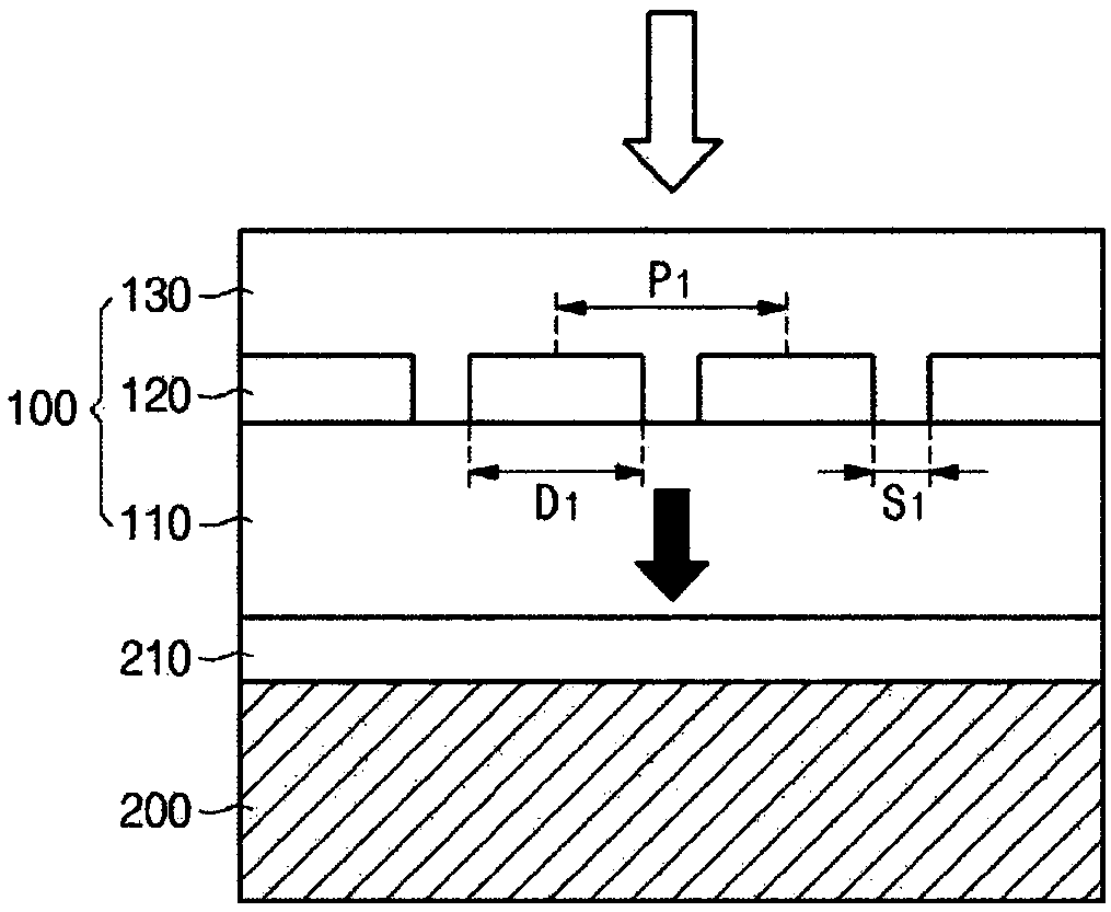
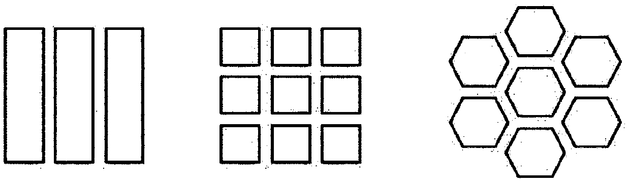
[0028] figure 1 is a diagram showing a cross section of an optical filter according to an embodiment of the present invention. figure 2 is a perspective view of an optical filter. image 3 is a diagram showing an example of a planar structure of a metal pattern.

[0029] The optical filter 100 includes a clad layer 110 , a plurality of metal patterns 120 patterned to have a periodic lattice structure, and an optical waveguide layer 130 formed on the plurality of metal patterns 120 . One of the features of the presen...


PUM


Abstract

The present invention provides an optical filter and an optical device using same, the optical filter comprising: a cladding layer; a plurality of metallic patterns regularly patterned on the claddinglayer; and an optical waveguide layer formed over the plurality of metallic patterns, wherein light proceeds from the optical waveguide layer to the cladding layer.

Description

technical field [0001] The present invention relates to an optical filter, and more particularly, to an optical filter and an optical device having an optical waveguide layer formed on a plurality of metal patterns. Background technique [0002] An optical filter is a configuration necessary to filter light having various wavelengths into an arbitrary wavelength band. Optical filters are used to configure miniature spectrometers since optical filters that transmit only light of a specific wavelength band or transmit light of different wavelength bands are integrated in an array. As a bandpass filter, a Fabry-Perot filter using the light interference effect of a dielectric resonator placed between two reflective films is typical. In addition, a transmission filter using an extraordinary optical transmission (EOT) phenomenon occurring in a nanohole array structure periodically arranged on a metal thin film structure is used. [0003] The advantage of the Fabry-Perot filter u...

Claims


Application Information

Patent Timeline
Patent Type & Authority Applications(China)
IPC IPC(8): G02B6/02G02B5/02G02B5/30
CPCG02B5/208G01J1/0488G01J1/0492G01J2001/0496G01J3/0259G01J3/1895G02B6/02057G02B5/0268G02B5/3058G02B6/12007G02B6/124G01J1/44G02B2006/12138G02B2006/12107G02B2006/12109
Inventor 李敬锡黄圭元金寅昊金元穆李旭圣郑斗硕
Owner SAMSUNG ELECTRONICS CO LTD
Why Eureka
Try Eureka