Touch control structure and preparation method thereof, and display device
A touch and non-touch technology, applied in the direction of oxide conductors, conductive layers on insulating carriers, plastic/resin/wax insulators, etc., can solve the problems that are prone to breakage, cannot meet the design requirements and functions of small curvature or folding products The problem of different layer stress
- Summary
- Abstract
- Description
- Claims
- Application Information
AI Technical Summary
Problems solved by technology
Method used
Image
Examples
preparation example Construction
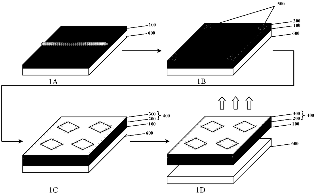
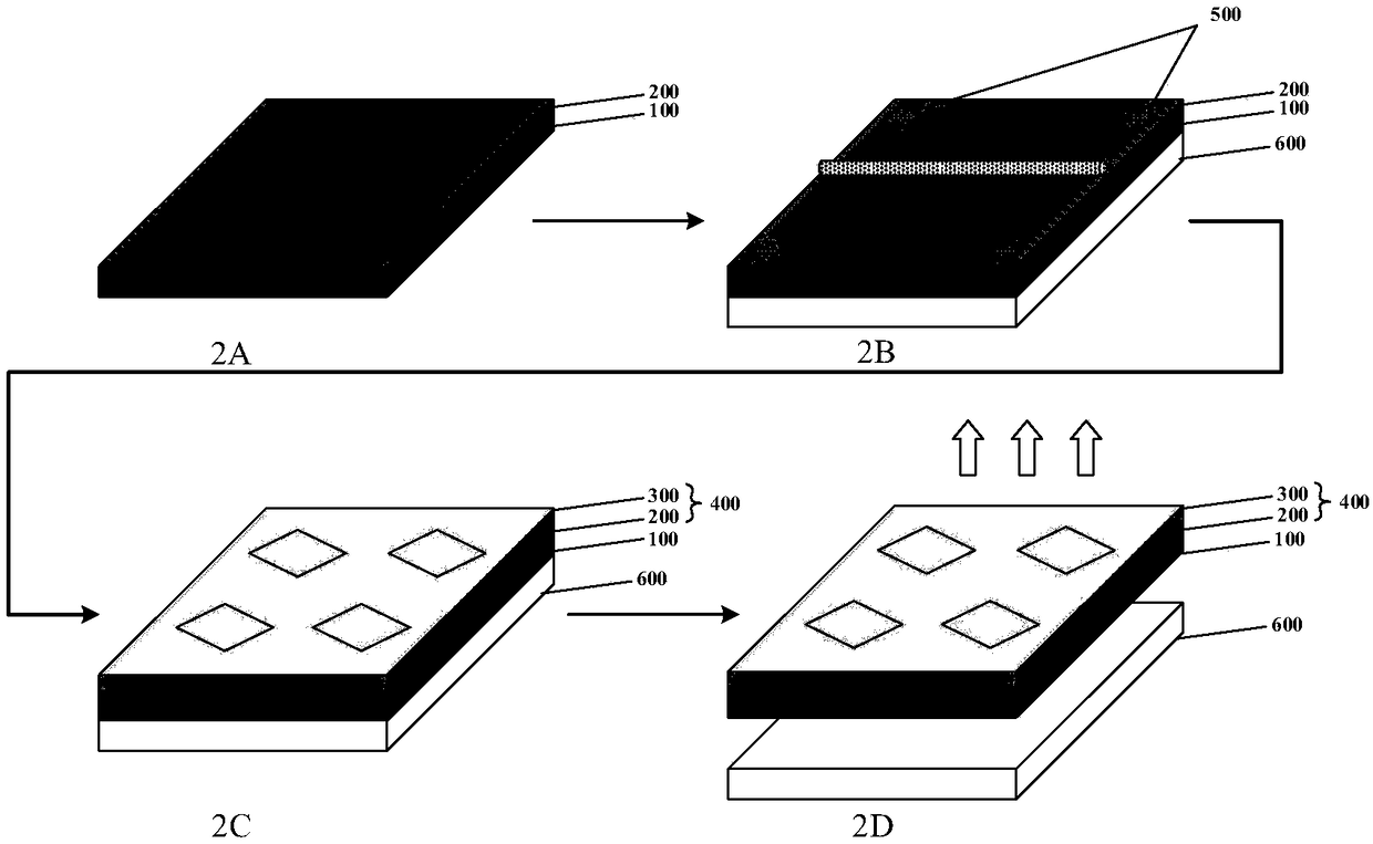
[0059] At least one embodiment of the present disclosure provides a method for manufacturing a touch structure, including: providing a film substrate; providing a base substrate, and attaching the film substrate to the base substrate; A stacked structure for realizing the touch function; and removing the film substrate on which the stacked structure is formed from the base substrate. At least one embodiment of the present disclosure further provides a touch control structure and a display device corresponding to the above-mentioned manufacturing method of the touch control structure.
[0060] The preparation method of the touch structure can make the functional layer of the touch structure distributed on the same side of the film substrate, and the stress is the same when it is bent, so that the risk of fracture can be reduced, and the preparation method can also improve the alignment accuracy.
[0061] In an embodiment of the present disclosure, the patterning process may be ...
Embodiment 1
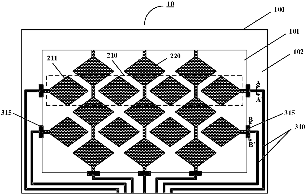
[0064] An example of this embodiment provides a touch structure, such as Figure 3A As shown, the touch structure 10 can be divided into a touch area 101 and a non-touch area 102 (for example, a peripheral area). For example, the touch area 101 is an area where touch electrodes are disposed, and the non-touch area 102 is an area where wires (such as metal wires) connected to the touch electrodes are disposed.
[0065] For example, also as figure 1 and figure 2 As shown, the touch structure 10 includes: a film substrate 100 ; a first conductive layer 200 disposed on the film substrate 100 ; and an alignment mark 500 disposed on the first conductive layer 200 for realizing the alignment function.
[0066] For example, the film substrate 100 adopts a film material with high transmittance, especially a film material with flexibility. For example, the film substrate 100 may be a cycloolefin polymer (COP) film or a polyimide (PI) film or the like. For another example, when the ...
Embodiment 2
[0099] This embodiment provides a display device, including the touch structure described in any one of the first embodiment.
[0100] The display device provided in this embodiment may also include a display screen. It should be noted that this embodiment does not limit the combination of the touch structure and the display screen.
[0101] For example, the display screen includes an array substrate and an opposite substrate (such as a color filter substrate) that is boxed with the array substrate.
[0102] For example, the touch control structure may be disposed on a protective cover, and the protective cover is used to cover the display screen to protect the display screen, and the side of the protective cover formed with the touch control structure faces the display screen. That is, the combination method of the touch structure and the display screen is an OGS (One Glass Solution) method.
[0103] For another example, the touch control structure may be disposed on a side...
PUM
 Abstract
Description
Claims
Application Information
 - R&D
- Intellectual Property
- Life Sciences
- Materials
- Tech Scout
- Unparalleled Data Quality
- Higher Quality Content
- 60% Fewer Hallucinations
Browse by: Latest US Patents, China's latest patents, Technical Efficacy Thesaurus, Application Domain, Technology Topic, Popular Technical Reports.
© 2025 PatSnap. All rights reserved.Legal|Privacy policy|Modern Slavery Act Transparency Statement|Sitemap|About US| Contact US: help@patsnap.com


