Image sensor and method of forming the same
A technology for image sensors and pixel areas, applied in semiconductor devices, electric solid devices, radiation control devices, etc., can solve problems such as poor performance of image sensors and light crosstalk
- Summary
- Abstract
- Description
- Claims
- Application Information
AI Technical Summary
Problems solved by technology
Method used
Image
Examples
Embodiment Construction
[0027] As mentioned in the background, prior art image sensors perform poorly.
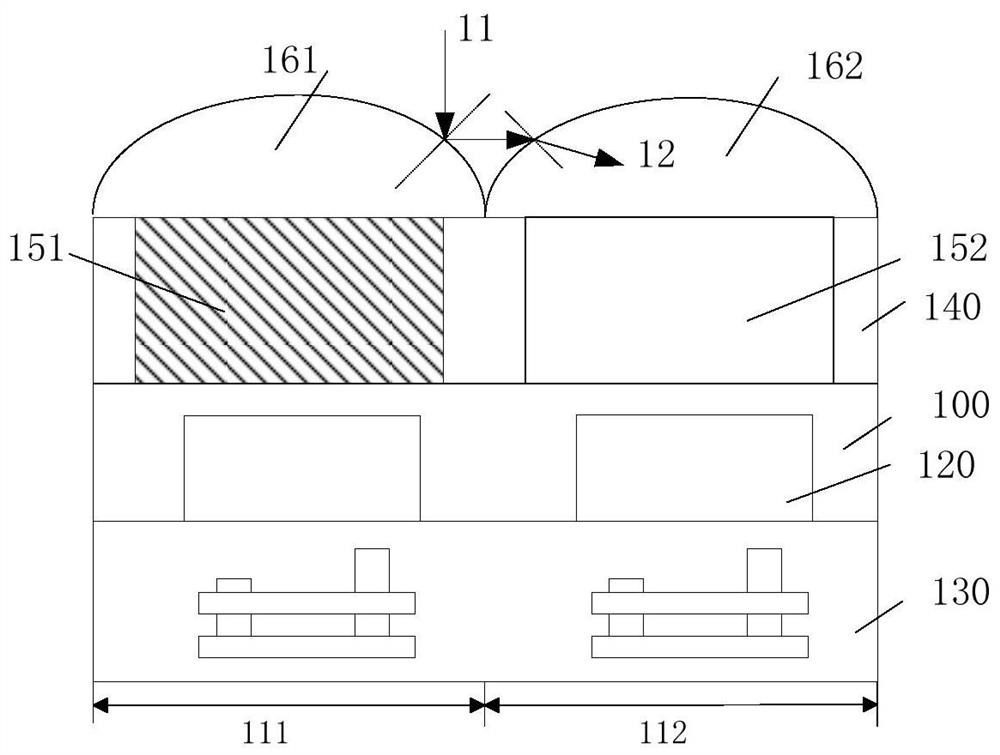
[0028] refer to figure 1 , figure 1 It is a structural schematic diagram of an image sensor. The image sensor includes a plurality of pixel areas, and the pixel area includes: a substrate 100, a photosensitive structure 120, an interconnection structure 130, and a light receiving structure. The substrate 100 has an opposite first surface and a second surface, the photosensitive structure 120 is located in the substrate 100, the photosensitive structure 120 is exposed on the first surface of the substrate 100, and the interconnect structure 130 is in contact with the first surface of the substrate 100; The light-receiving structure is located on the second surface of the substrate 100, and the light-receiving structure includes a lens layer, a filter layer and a grid layer 140, the lens layer is located on the surface of the filter layer, and the grid layer 140 is located between adjacent filter l...
PUM
 Abstract
Description
Claims
Application Information
 - R&D
- Intellectual Property
- Life Sciences
- Materials
- Tech Scout
- Unparalleled Data Quality
- Higher Quality Content
- 60% Fewer Hallucinations
Browse by: Latest US Patents, China's latest patents, Technical Efficacy Thesaurus, Application Domain, Technology Topic, Popular Technical Reports.
© 2025 PatSnap. All rights reserved.Legal|Privacy policy|Modern Slavery Act Transparency Statement|Sitemap|About US| Contact US: help@patsnap.com


