One-dimensional photonic crystal sun-blind ultraviolet bandpass filter
A three-dimensional photonic crystal and photonic crystal technology, applied in the optical field, can solve the problems of low transmittance and little improvement in the filtering performance of solar-blind ultraviolet filter devices.
- Summary
- Abstract
- Description
- Claims
- Application Information
AI Technical Summary
Problems solved by technology
Method used
Image
Examples
Embodiment 1
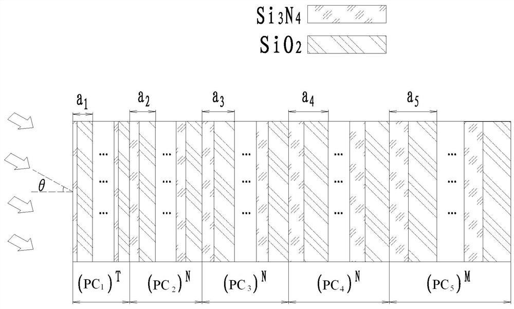
[0021] Such as figure 1 As shown, embodiment 1 of the present invention provides a kind of one-dimensional photonic crystal sun-blind ultraviolet bandpass filter, and its quantum well structure is successively increased by five kinds of photonic crystal PC of lattice constant 1 , PC 2 , PC 3 , PC 4 , PC 5 Stacked sequentially, the five photonic crystals are formed by periodic arrangement of high-refractive-index material layers and low-refractive-index material layers; in each photonic crystal, the thickness of the high-refractive-index material layer is equal, and the low-refractive-index material layer is The same thickness; the photonic crystal PC 1 The period is 6, the photonic crystal PC 2 , PC 3 , PC 4 The period is 5, the photonic crystal PC 5 The period is 6.
[0022] Based on the frequency domain superposition principle, the bandpass photonic crystal filter with quantum well structure can be expressed as (PC 1 ) T (PC 2 ) N (PC 3 ) N(PC 4 ) N (PC 5 )...
Embodiment 2
[0029] Same as Embodiment 1, the one-dimensional photonic crystal sun-blind ultraviolet band-pass filter provided by Embodiment 2 of the present invention has a quantum well structure of five photonic crystal PCs whose lattice constants are sequentially increased. 1 , PC 2 , PC 3 , PC 4 , PC 5 These five kinds of photonic crystals are formed by periodic arrangement of high-refractive-index material layers and low-refractive-index material layers; in each photonic crystal, the thickness of the high-refractive-index material layer is equal, and the thickness of the low-refractive-index material layer is The thickness is the same, and its specific thickness is as shown in Table 1, and the photonic crystal PC 1 The period is 6; different from embodiment 1, in this embodiment, the photonic crystal PC 2 , PC 3 , PC 4 The period is 3~6, the photonic crystal PC 5 The period is 10.
[0030] Such as Figure 6 As shown, the three photonic crystal PCs in the middle 2 , PC 3 ,...
PUM
| Property | Measurement | Unit |
|---|---|---|
| thickness | aaaaa | aaaaa |
| thickness | aaaaa | aaaaa |
| wavelength | aaaaa | aaaaa |
Abstract
Description
Claims
Application Information
 - Generate Ideas
- Intellectual Property
- Life Sciences
- Materials
- Tech Scout
- Unparalleled Data Quality
- Higher Quality Content
- 60% Fewer Hallucinations
Browse by: Latest US Patents, China's latest patents, Technical Efficacy Thesaurus, Application Domain, Technology Topic, Popular Technical Reports.
© 2025 PatSnap. All rights reserved.Legal|Privacy policy|Modern Slavery Act Transparency Statement|Sitemap|About US| Contact US: help@patsnap.com


