Reaction chambers and semiconductor processing equipment

A reaction chamber and process technology, used in semiconductor/solid-state device manufacturing, electrical components, circuits, etc., can solve problems such as high processing accuracy and cost, increase equipment complexity, etc., achieve simple structure, solve long cleaning and maintenance cycles, Easy to process effect

Active Publication Date: 2021-10-15
BEIJING NAURA MICROELECTRONICS EQUIP CO LTD
View PDF9 Cites 0 Cited by
  • Summary
  • Abstract
  • Description
  • Claims
  • Application Information

AI Technical Summary

Problems solved by technology

However, the double-layer Faraday shield increases the complexity of the equipment, and the processing accuracy and cost are high

Method used


Image

  • Reaction chambers and semiconductor processing equipment
  • Reaction chambers and semiconductor processing equipment
  • Reaction chambers and semiconductor processing equipment

Examples


Embodiment Construction

[0028] In order to enable those skilled in the art to better understand the technical solutions of the present invention, the reaction chamber and semiconductor processing equipment of the present invention will be further described in detail below with reference to the drawings and specific implementation methods.

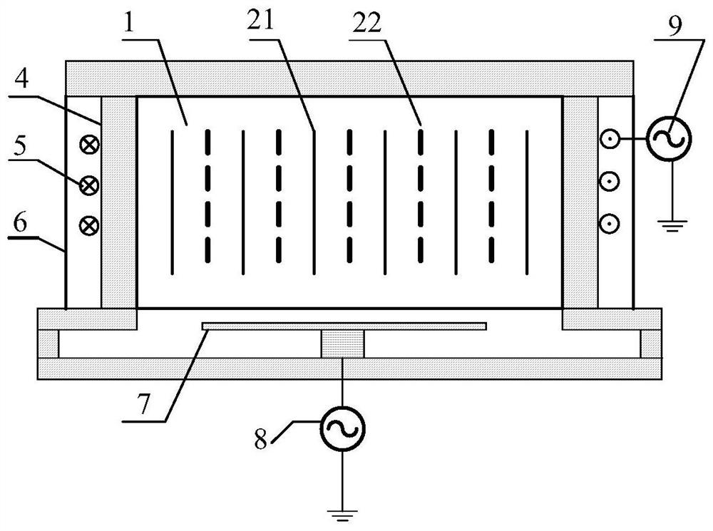
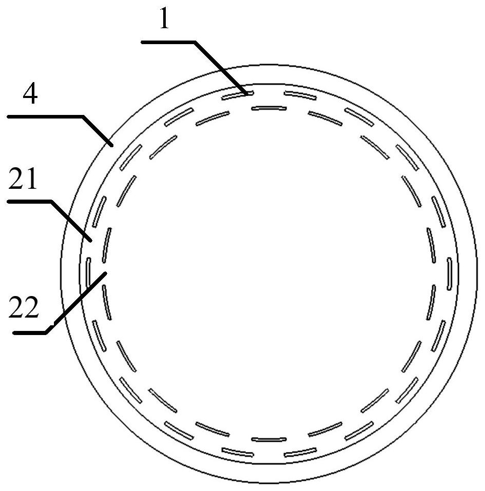
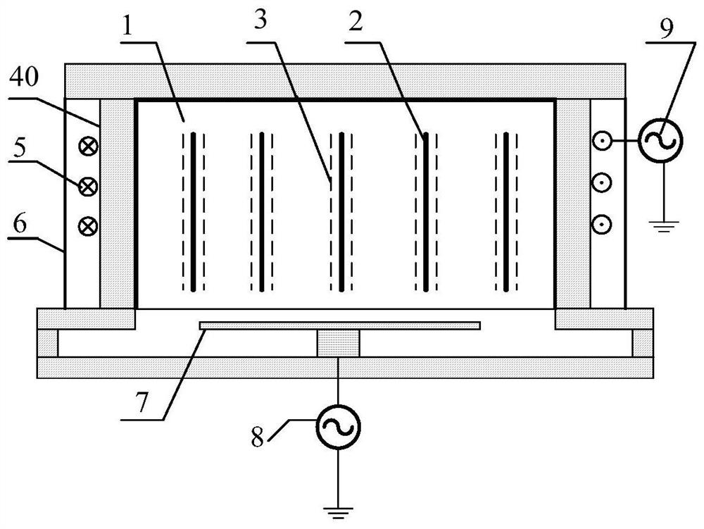
[0029] This embodiment provides a reaction chamber, the reaction chamber includes a vacuum-sealed barrel and a Faraday shield embedded in the vacuum-sealed barrel, the Faraday shield is provided with a slit running through the thickness of the Faraday shield, wherein the vacuum-sealed barrel The inner wall of the inner wall is provided with a recess at a region corresponding to the slit, and the recess is used to accommodate process by-products from the slit of the Faraday shield. In the reaction chamber, a recess is formed on the inner wall of the vacuum-sealed barrel to form an accommodating space for by-products deposited on the vacuum-sealed barrel during the p...


PUM

PropertyMeasurementUnit
depthaaaaaaaaaa

Abstract

The invention belongs to the technical field of semiconductor processing, and in particular relates to a reaction chamber and semiconductor processing equipment. The reaction chamber includes a vacuum-sealed barrel and a Faraday shield embedded in the vacuum-sealed barrel, the Faraday shield is provided with a slit running through its thickness, and the inner wall of the vacuum-sealed barrel is opened at a region corresponding to the slit. A recess for containing process by-products from the opening of the Faraday shield. The structure of the reaction chamber is simpler, and the processing is easier. Since the recess can accommodate the process by-products from the slit of the Faraday shield, it effectively solves the problem of long cleaning and maintenance cycles of the vacuum sealed barrel, and under the same conditions The coupling efficiency of electromagnetic energy and plasma is higher; correspondingly, the semiconductor processing equipment formed on this basis has a longer cleaning and maintenance cycle and better processing effect.

Description

technical field [0001] The invention belongs to the technical field of semiconductor processing, and in particular relates to a reaction chamber and semiconductor processing equipment. Background technique [0002] The Faraday shield is often used in the precleaning (Preclean) device of the inductively coupled plasma to reduce the capacitive coupling components of the plasma and increase the plasma density. Especially when etching (sputtering) a wafer coated with a metal (Metal) film, the Faraday shield is an essential component, and also plays a role in reducing metal deposition on the ceramic tub (Ceramic tub). [0003] Typically, the Faraday shield is provided with multiple slots to reduce eddy current losses and allow electromagnetic field energy to couple into the plasma. The sputtered metal particles can pass through the slits of the Faraday shield and deposit on the ceramic barrel, forming a thin film between the slits. When the metal film reaches a certain thicknes...

Claims


Application Information

Patent Timeline
Patent Type & Authority Patents(China)
IPC IPC(8): H01L21/67
CPCH01L21/67213
Inventor 王文章陈鹏
Owner BEIJING NAURA MICROELECTRONICS EQUIP CO LTD
Why Eureka
Try Eureka