Level shifting structure and manufacturing method thereof

A technology of level shift and drift region, which is applied in semiconductor/solid-state device manufacturing, circuits, electrical components, etc., can solve problems such as ultra-high voltage NDLDMOS reliability problems, difficult process control, large drift region size, etc., and achieves leakage isolation Good effect, easy process control, uniform doping concentration distribution

Active Publication Date: 2018-09-04
SHANGHAI HUAHONG GRACE SEMICON MFG CORP
View PDF14 Cites 1 Cited by
  • Summary
  • Abstract
  • Description
  • Claims
  • Application Information

AI Technical Summary

Problems solved by technology

There are two problems with this structure. First, the drift region size of the level-shift structure using the Double RESURF effect is relatively large, and shortening the drift region size will cause excessive electric field and cause reliability problems of ultra-high voltage NDLDMOS.
Second, two upper and lower P-implants are used to realize the through-connection through thermal process diffusion, and isolate the level-shift structure and the high-side area. This method will cause the upper and lower two-layer connection parts to be narrow in the middle and wide at both ends, as shown in the dotted line box 204 in Figure 1. As shown, in the isolation potential, the narrower part is easy to be depleted first, which will cause a series leakage. If the narrow part is widened, the two ends will be wider. Process control is more difficult

Method used


Image

  • Level shifting structure and manufacturing method thereof
  • Level shifting structure and manufacturing method thereof

Examples


Embodiment Construction

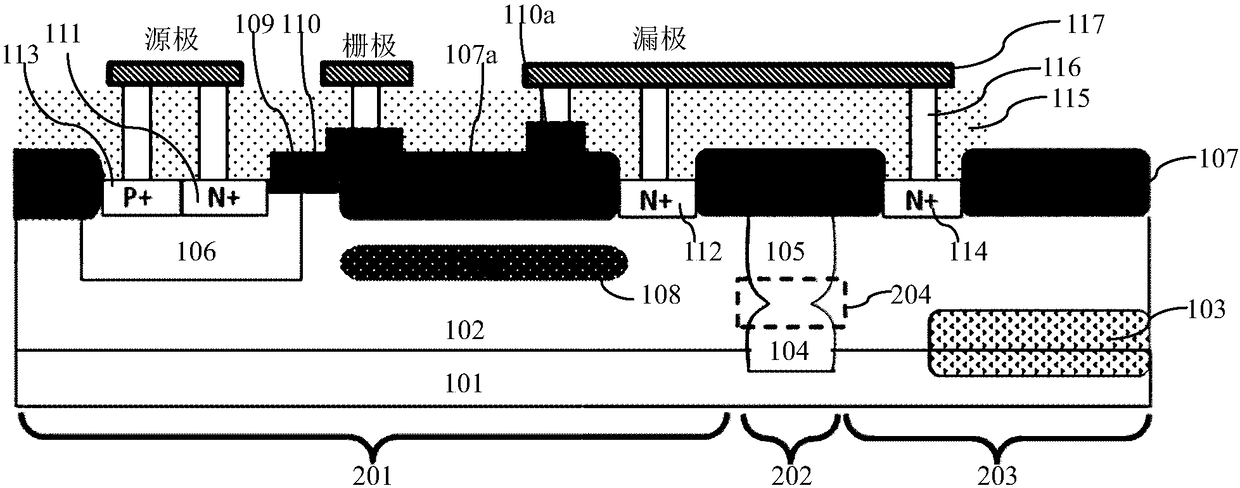
[0057] Such as figure 2 As shown, it is a schematic structural diagram of the level shift structure of the embodiment of the present invention. The level shift structure of the embodiment of the present invention includes: LDMOS301, through isolation region 302 and high side region 303, and the through isolation region 302 displaces the LDMOS301 and between the high side area 303 .

[0058] A first epitaxial layer 2 of a first conductivity type is formed on a surface of a semiconductor substrate of a second conductivity type, such as a silicon substrate 1 .

[0059] The first buried layer 4 with the second conductivity type is formed at the interface of the semiconductor substrate 1 and the first epitaxial layer 2 in the via isolation region 302 .

[0060] The second buried layer 3 with the first conductivity type is formed at the interface of the semiconductor substrate 1 and the first epitaxial layer 2 in the high side region 303 .

[0061] The body region 6 of the LDMOS ...


PUM

PropertyMeasurementUnit
Widthaaaaaaaaaa
Spacingaaaaaaaaaa

Abstract

The present invention discloses a level shifting structure. The level shifting structure includes an LDMOS, a pass isolation region and a high side region; the pass isolation region includes a first buried layer having a second conductivity type and a second well region having a second conductivity type, wherein the second well region is connected to the bottom first buried layer; a drift region of the LDMOS is composed of a first epitaxial layer, and drift region field oxygen is formed on a surface of the drift region; a surface electric field reduction structure is formed in the drift regionon the bottom of the drift region field oxygen, the surface electric field reduction structure comprises two or more second conductivity type injection layers; the injection depth of the second conductivity type injection layer on the bottommost layer is equal to a connection position between the second well region and the first buried layer, and a third injection region is superimposed at the connection position and is formed simultaneously with the bottommost second conductivity type injection layer. The invention discloses a manufacturing method for the level shifting structure. The invention can reduce the leakage of the pass isolation region while enhancing the effect of reducing the surface electric field and reducing the on-resistance.

Description

technical field [0001] The invention relates to the field of semiconductor integrated circuit manufacturing, in particular to a level shifting structure; the invention also relates to a manufacturing method of an NLDMOS device. Background technique [0002] In the current high-voltage integrated circuit (HVIC) process, in order to realize high-side and low-side driving, a high-voltage isolation ring is required so that the high-side can be directly connected to the mains. This area needs to be able to withstand high voltages above 600V, and at the same time requires a level shift The structure converts the high voltage of the mains power into a low voltage and transmits it to the low side to supply power to the low side circuit. [0003] In the prior art, LDMOS is usually used to implement a level shift structure, such as figure 1 Shown is a structural schematic diagram of the existing level shifting structure, figure 1 Taking N-type LDMOS (NLDMOS) as an example for illust...

Claims


Application Information

Patent Timeline
IPC IPC(8): H01L29/78H01L29/06H01L21/336
CPCH01L29/0634H01L29/66681H01L29/7816H01L29/42368H01L29/402
Inventor 苗彬彬
Owner SHANGHAI HUAHONG GRACE SEMICON MFG CORP
Why Eureka
Try Eureka