Electric moistening display and producing method thereof
An electrowetting display and manufacturing method technology, applied in the direction of instruments, optical components, optics, etc., can solve the problems of high parallelism requirements, large equipment footprint, unsuitable for flexible display devices, etc., and achieve good filling uniformity , avoid the phenomenon of overturning the wall, and ensure the effect of the distance between boxes
- Summary
- Abstract
- Description
- Claims
- Application Information
AI Technical Summary
Problems solved by technology
Method used
Image
Examples
Embodiment 1
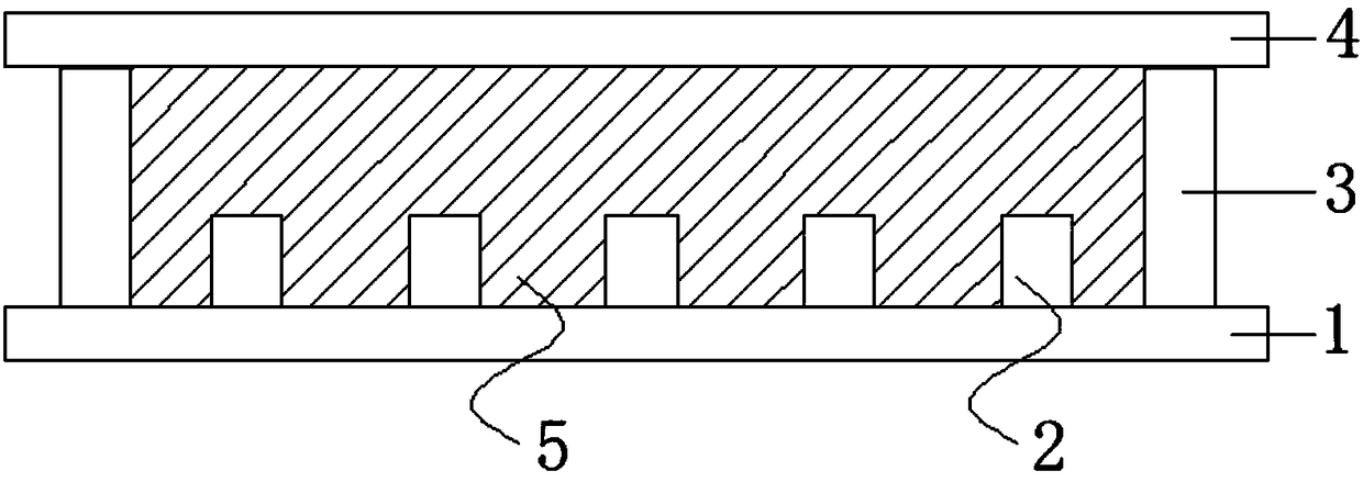
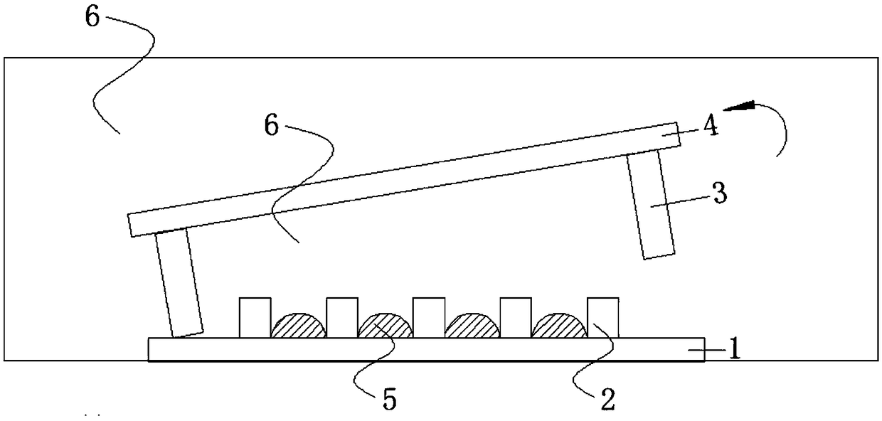
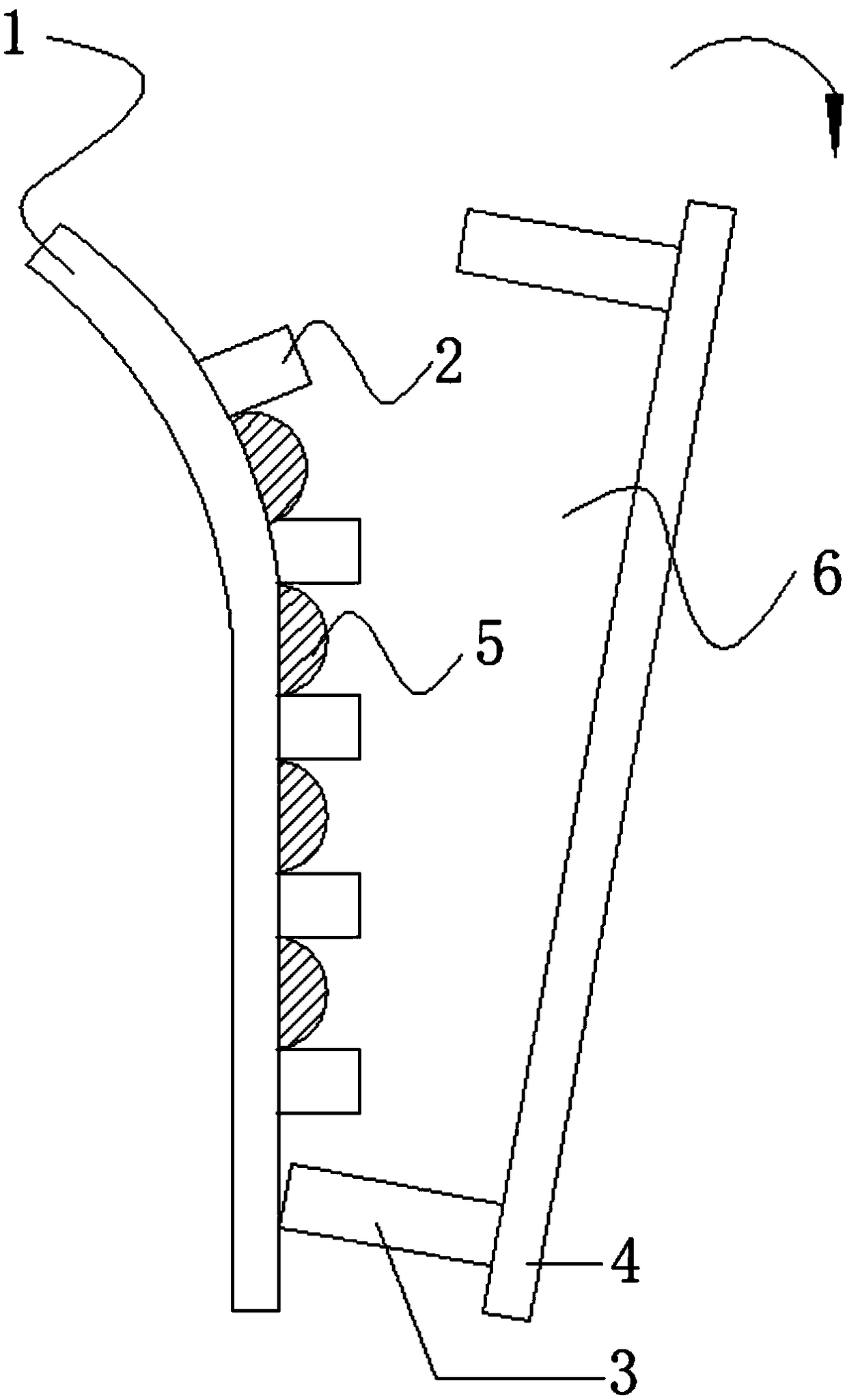
[0031] The invention provides a method for manufacturing an electrowetting display, comprising the following steps:
[0032] Take off the substrate, the lower substrate includes a substrate, a conductive layer and an insulating layer arranged in sequence, and the substrate can be a rigid substrate such as glass, or a flexible substrate such as a PET plate, a PEN plate, a PI plate; the conductive layer can be It is an ITO conductive layer or a PI conductive layer; the insulating layer can be a layer of hydrophobic insulating layer material, or a composite layer obtained by adding a layer of hydrophobic coating on the surface of the insulating material, such as silicon dioxide, silicon nitride, organic Spin-coat hydrophobic layer materials on the surface of insulating materials such as insulating materials. The hydrophobic layer materials mainly include DuPont’s AF fluororesin series (such as AF1600), CYTOP fluororesin from Japan’s Asahi Whistle, and Solvay’s Hyflon fluororesin. ...
Embodiment 2
[0039] The invention provides a method for manufacturing an electrowetting display, comprising the following steps:
[0040] Take the substrate, the substrate material of the lower substrate is a flexible substrate PET board, and then prepare a pixel wall on the lower substrate, the pixel wall encloses a pixel grid, the length of the bottom surface of the pixel grid: width = 1.5: 1, the The height of the pixel grid: the length of the pixel grid=2:1. In the present invention, the shape of the bottom surface of the pixel grid can be a rectangle, preferably the length of the bottom surface: width = (1.5-2):1.
[0041] Preparation of filling plate: take a hydrophilic glass substrate, use acrylic UV-curable glue to stick a PET frame on the hydrophilic glass substrate, the area of the PET frame is larger than the area surrounded by the pixel wall, and the thickness of the PET frame is 100 μm.
[0042] Fill the pixel grid with ink with a concentration of 30%, and cover the filling...
PUM
| Property | Measurement | Unit |
|---|---|---|
| Thickness | aaaaa | aaaaa |
| Viscosity | aaaaa | aaaaa |
| Viscosity | aaaaa | aaaaa |
Abstract
Description
Claims
Application Information
 - R&D
- Intellectual Property
- Life Sciences
- Materials
- Tech Scout
- Unparalleled Data Quality
- Higher Quality Content
- 60% Fewer Hallucinations
Browse by: Latest US Patents, China's latest patents, Technical Efficacy Thesaurus, Application Domain, Technology Topic, Popular Technical Reports.
© 2025 PatSnap. All rights reserved.Legal|Privacy policy|Modern Slavery Act Transparency Statement|Sitemap|About US| Contact US: help@patsnap.com


