


Quick Research
Generate reliable direction feasibility study reports for your R&D in just a few steps.

Technical Q&A
Discover and master advanced knowledge NOW. Basics, ideas, possibilities, all at once.

Find Solutions
As an expert in R&D theories, this can generate solutions to your technical problems instantly.

Evaluate Feasibility
Analyze your overall solution with one click, know your potential R&D risks in advance.

Monitor Landscape
Get weekly tech updates, stay abreast of the latest tech innovations and key insights.
A connection probe, its preparation method and use in microelectrode array connection
A technology for connecting probes and connecting columns, which is applied in the directions of electrodes, internal electrodes, and head electrodes, etc., which can solve the problems of affecting the performance and life of the microelectrode array, damaging the welding end of the microelectrode array, increasing the difficulty and cost of production, etc. Achieve the effect of reversible connection mode, good universality and wide range
- Summary
- Abstract
- Description
- Claims
- Application Information
AI Technical Summary
Problems solved by technology
Method used
Image

Examples
Embodiment 1
[0073] This embodiment provides a ligation probe and a preparation method thereof, the method comprising:
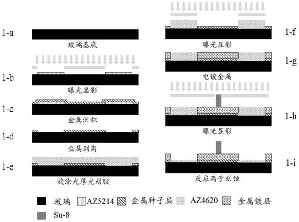
[0074] (1) Prepare the substrate: select a glass sheet with better dielectric properties as the substrate, and use it after cleaning (see figure 1 1-a) in.
[0075] (2) Exposure and development: Spin-coat a layer of photoresist AZ5214 on the substrate with a thickness of 3-5 microns. After heating and curing, use the first layer of mask as a mask for exposure and development (see figure 1 1-b) in.
[0076] (3) Metal deposition and metallic glass: the metal coating process is carried out on the sample after photolithography, and the Cr / Au metal layer of 20nm / 100nm is completed, and the target metal pattern is obtained by lift-off (see figure 1 1-c and 1-d in )
[0077] (4) Spin-coat light-thick photoresist, exposure and development, and electroplating metal: Next, spin-coat AZ4620 photoresist of 7-8 microns, expose and develop the metal of the probe part, and use the t...
Embodiment 2
[0082] Except not carrying out step (5) the step of spin-coating SU-8, other methods and conditions are identical with embodiment 1.
Embodiment 3
[0084] This embodiment provides a ligation probe and a preparation method thereof, the method comprising:
[0085] (1) Spin-coat AZ5214 photoresist with a thickness of 3 μm on the substrate, heat and cure it, then use a mask for exposure and development, and then deposit a 20nm Cr layer and a 100nm Au layer on the entire substrate area successively. This 120nm thick composite layer As a metal seed layer, the photoresist is stripped to form a metal seed layer arranged at intervals on the substrate;
[0086](2) Spin-coat AZ4620 photoresist on the entire substrate area, then expose the metal seed layer by exposure and development, use the photoresist as a mask, and electroplate on the metal seed layer to obtain a 7 μm thick metal coating, the metal seed layer and The metal plating layers jointly form array units arranged at intervals;
[0087] Wherein, the thickness of the AZ4620 photoresist is 7 μm to 8 μm, which is the same as the thickness of the array unit;
[0088] (2)'Spi...
PUM
| Property | Measurement | Unit |
|---|---|---|
| diameter | aaaaa | aaaaa |
| thickness | aaaaa | aaaaa |
| thickness | aaaaa | aaaaa |
Abstract
Description
Claims
Application Information
 - R&D Engineer
- R&D Manager
- IP Professional
- Industry Leading Data Capabilities
- Powerful AI technology
- Patent DNA Extraction
Browse by: Latest US Patents, China's latest patents, Technical Efficacy Thesaurus, Application Domain, Technology Topic, Popular Technical Reports.
© 2024 PatSnap. All rights reserved.Legal|Privacy policy|Modern Slavery Act Transparency Statement|Sitemap|About US| Contact US: help@patsnap.com