Silicon crystal detection method and device

A detection method and detection device technology, which is applied in the direction of measuring devices, semiconductor/solid-state device testing/measurement, and material analysis, can solve the problems of increasing costs and energy consumption, and achieve the effect of quick learning

Inactive Publication Date: 2018-06-08
AUO CRYSTAL
View PDF3 Cites 0 Cited by
  • Summary
  • Abstract
  • Description
  • Claims
  • Application Information

AI Technical Summary

Problems solved by technology

However, increasing the optical power of the laser light source consumes energy and increases costs

Method used


Image

  • Silicon crystal detection method and device
  • Silicon crystal detection method and device
  • Silicon crystal detection method and device

Examples


no. 1 example

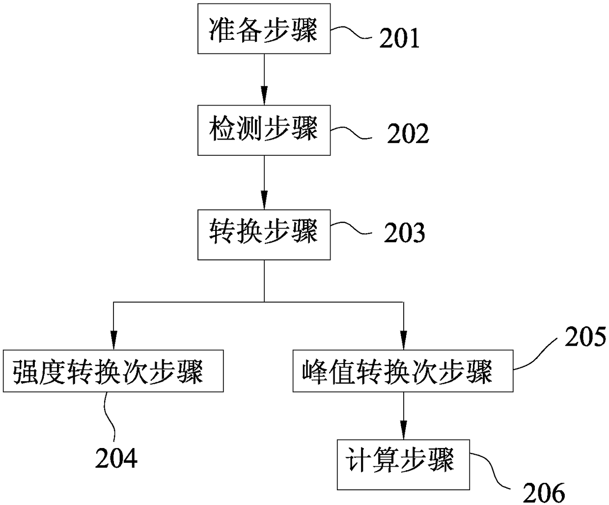
[0037] refer to figure 1 , a first embodiment of the detection method for silicon crystal material of the present invention includes a preparation step 201 , a detection step 202 , a conversion step 203 , and a calculation step 206 .

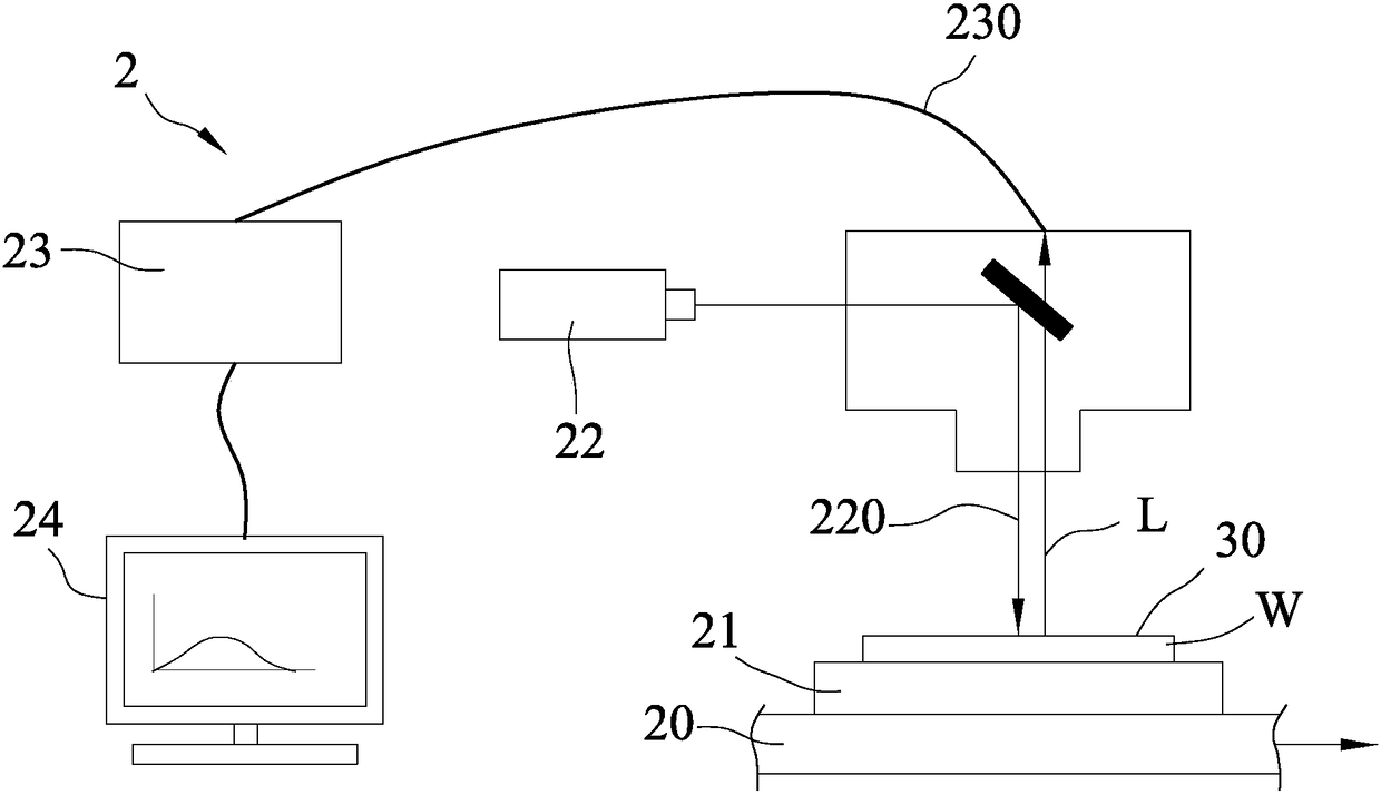
[0038] Cooperate with reference figure 2 , first perform the preparation step 201 , prepare a detection device 2 , and set a silicon crystal material to be detected on the detection device 2 .

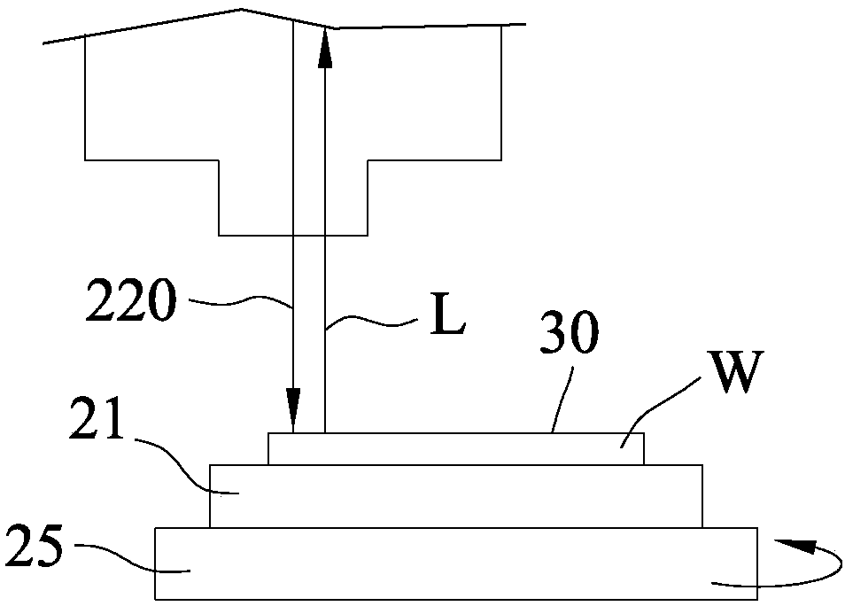
[0039] Specifically, the detection device 2 includes a stage 21 arranged on a slide rail 20 and capable of moving along a predetermined path of the silicon crystal material, a laser 22 capable of emitting a laser light source 220, a light receiving The light receiver 23 of the component 230, and an operation display 24. Specifically, the silicon crystal material can be a polycrystalline silicon ingot, a single crystal silicon ingot, a polycrystalline wafer, or a single crystal wafer. In this embodiment, the silicon crystal material is a single crystal...

specific example 1

[0054] A specific example 1 of the silicon crystal material detection method of the present invention is the silicon crystal material detection method of the first embodiment, and the intensity conversion sub-step 204 to the conversion step 203 is performed.

[0055] Cooperate with reference figure 1 and figure 2 , a single crystal wafer W 1 (not shown in the figure) is arranged on the stage 21, and uses a laser light source 220 with a wavelength of 808nm and a wattage of 1W close to the energy gap (band gap) of silicon to radially (for example, a single crystal wafer) diagonal, but not limited thereto, in other embodiments it can also be half of the diagonal) a single point multiple times to irradiate the single crystal wafer W 1 on the surface of the surface, making it produce multiple photoluminescence L. Next, use a spectrometer as the light receiver 23 to receive the photoluminescent light L, and generate a plurality of photoluminescent signals corresponding to the ph...

specific example 2

[0057] The implementation conditions of a specific example 2 of the silicon crystal material detection method of the present invention are substantially the same as the specific example 1, the difference is that the specific example 2 is to detect another single crystal wafer different from the specific example 1 W 2 (not shown).


PUM

PropertyMeasurementUnit
wavelengthaaaaaaaaaa

Abstract

The invention discloses a silicon crystal detection method, and the method comprises a preparation step and a detection step. The preparation step is a step of preparing a detection device which comprises a carrying table, a laser light source and a light receiver, and placing a to-be-detected silicon crystal on the carrying table. The detection step is a step of enabling the laser light source toirradiate the surface of the silicon crystal at a predetermined wavelength along at least one predetermined path of the silicon crystal, and enabling the silicon crystal to generate a plurality of photoinduced fluorescent light beams activated by the laser light source along the predetermined path, wherein the light receiver can receive the photoinduced fluorescent light beams and generates a plurality of corresponding photoinduced fluorescent light beam signals. The laser light source is used for irradiating the silicon crystal along the predetermined path to generate the plurality of photoinduced fluorescent light beams, and the plurality of corresponding photoinduced fluorescent light beam spectrums corresponding to the predetermined path are obtained, thereby obtaining the fluorescentlight intensity distribution of the silicon crystal through backstepping, and obtaining the quality of the silicon crystal. In addition, the invention also provides a silicon crystal detection device.

Description

technical field [0001] The invention relates to a detection method and device for a silicon crystal material, in particular to a detection method and a detection device for irradiating the surface of a silicon crystal material with a point light source along a predetermined path. Background technique [0002] The existing method for detecting polysilicon wafers is mainly to uniformly irradiate a high-power laser light source on a whole wafer to be tested through spectroscopic technology, so that the wafer to be tested produces fluorescent light excited by the laser light source. , and then through a camera device arranged on the wafer to be tested, to receive the fluorescent light generated by the entire wafer to be tested, to know the intensity distribution of the wafer to be tested, so as to judge the wafer to be tested the quality of. [0003] The aforementioned detection method needs to make the laser light source have a high optical power, so that the laser light sourc...

Claims


Application Information

Patent Timeline
Patent Type & Authority Applications(China)
IPC IPC(8): G01N21/64H01L21/66
CPCG01N21/6402G01N21/6456H01L22/12
Inventor 陈宥菘侯语辰李立婷
Owner AUO CRYSTAL
Why Eureka
Try Eureka