Glass substrate wiring structure, glass substrate and display device

A glass substrate and wiring structure technology, which is applied in the field of liquid crystal display, can solve the problems that the wiring resistance cannot be improved, the wiring space is limited, and the charging effect of the glass substrate cannot be improved, so as to achieve the effect of improving the charging effect and reducing the wiring resistance

Inactive Publication Date: 2018-01-19
SHENZHEN CHINA STAR OPTOELECTRONICS SEMICON DISPLAY TECH CO LTD
View PDF4 Cites 1 Cited by
  • Summary
  • Abstract
  • Description
  • Claims
  • Application Information

AI Technical Summary

Problems solved by technology

[0003] like figure 1 As shown, in the TFT glass substrate manufacturing process of high-ppi displays, the connection between the multiplexer MUX and the integrated circuit IC is basically connected by a plurality of connection lines a with equal spacing and equal line width. However, due to the limitation of MUX and IC The wiring space between them, the wiring resistance has been unable to be improved, resulting in the inability to improve the charging effect of the glass substrate

Method used


Image

  • Glass substrate wiring structure, glass substrate and display device
  • Glass substrate wiring structure, glass substrate and display device

Examples


Embodiment Construction

[0020] In order to make the object, technical solution and advantages of the present invention clearer, the present invention will be further described in detail below in conjunction with the accompanying drawings.

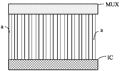
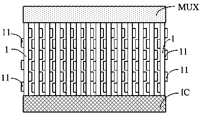
[0021] Such as figure 2 As shown, in Embodiment 1 of the present invention, a wiring structure of a glass substrate is provided, used between the demultiplexer MUX and the integrated circuit IC, including a plurality of connection lines 1, and the two ends of each connection line 1 are connected to MUX and IC, and a preset distance is reserved between any two adjacent connecting lines 1; where,

[0022] At least one connecting wire 1 is provided with one or more conductive protruding teeth 11, and each protruding tooth 11 on any connecting wire 1 is connected with its adjacent connecting wire 1 or each protruding tooth on the adjacent connecting wire 1 There is also a certain distance reserved between 11.

[0023] It can be understood that the convex tooth 11 o...


PUM


Abstract

The invention provides a glass substrate wiring structure used between a multiplexer (MUX) and an integrated circuit (IC). The glass substrate wiring structure comprises a plurality of connecting lines. The two ends of each connecting line are connected with the MUX and the IC respectively. A preset space is reserved between any two adjacent connecting lines. At least one connecting line is provided with one or more conductive protruding teeth. A certain distance is reserved between each protruding tooth on any connecting line and the adjacent collecting line or between each protruding tooth on any connecting line and each protruding tooth on the adjacent connecting line. The invention further provides a glass substrate and a display device. Wiring resistance can be reduced in existing limited wiring space, and the charging effect of the glass substrate is improved.

Description

technical field [0001] The invention relates to the technical field of liquid crystal display, in particular to a wiring structure of a glass substrate, a glass substrate and a display device. Background technique [0002] With the development of the flat-panel display industry, modern people continue to put forward higher requirements for the fineness of display quality. Choosing a high-ppi (Pixels per Inch, including the number of pixels per inch) display has become a digital electronic product. Standard configuration. [0003] Such as figure 1 As shown, in the TFT glass substrate manufacturing process of high-ppi displays, the connection between the multiplexer MUX and the integrated circuit IC is basically connected by a plurality of connection lines a with equal spacing and equal line width. However, due to the limitation of MUX and IC Between the wiring space, the wiring resistance has not been improved, resulting in the inability to improve the charging effect of th...

Claims


Application Information

Patent Timeline
Patent Type & Authority Applications(China)
IPC IPC(8): G02F1/1345
CPCH01L2924/14H01L2924/15788G02F1/13452H01L24/49H01L2924/17788
Inventor 吴焕达
Owner SHENZHEN CHINA STAR OPTOELECTRONICS SEMICON DISPLAY TECH CO LTD
Why Eureka
Try Eureka