
Amoled image processing method, driver chip and wearable device

An image processing and background image technology, applied in image data processing, image enhancement, image analysis, etc., can solve the problems of edge aliasing, etc., achieve the effect of reducing brightness and contrast, weakening edge aliasing, and enhancing customer experience

Active Publication Date: 2019-11-05
BOE TECH GRP CO LTD +1
View PDF4 Cites 0 Cited by
  • Summary
  • Abstract
  • Description
  • Claims
  • Application Information

AI Technical Summary

Problems solved by technology

[0005] In view of this, an embodiment of the present invention provides an AMOLED image processing method, a driver chip, and a wearable device to solve the edge jaggedness problem of the existing AMOLED in non-rectangular display

Method used


Image

  • Amoled image processing method, driver chip and wearable device
  • Amoled image processing method, driver chip and wearable device
  • Amoled image processing method, driver chip and wearable device

Examples


Embodiment Construction

[0054] The specific implementations of the AMOLED image processing method, driving chip, and wearable device provided by the embodiments of the present invention will be described in detail below with reference to the accompanying drawings.

[0055] The shapes and sizes of the components in the drawings do not reflect the true proportions, and are only intended to illustrate the content of the present invention schematically.

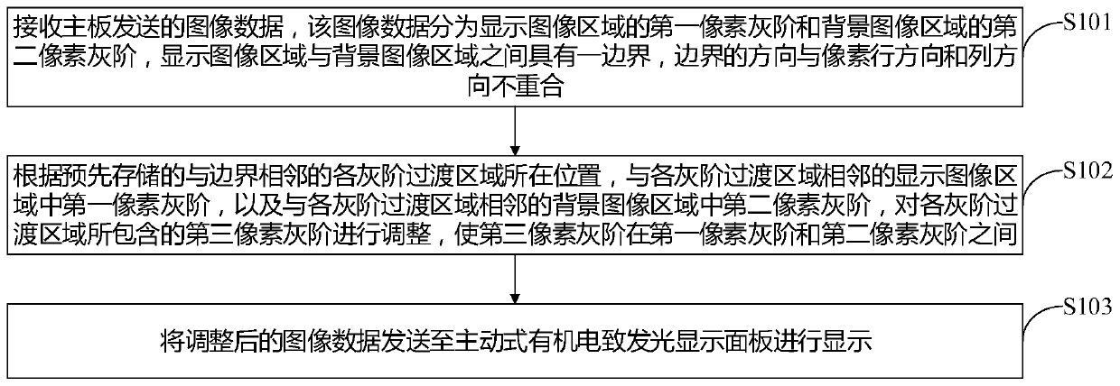
[0056] Specifically, in view of the problem that the existing active organic electroluminescence display panel displays a non-rectangular image area, serious jaggedness appears at the edge of the display, an active organic electroluminescence display panel provided by an embodiment of the present invention The image processing method of the display panel, such as figure 1 As shown, the following steps can be specifically included:

[0057] S101. Receive image data sent by the main board. The image data is divided into a first pixel gray scale in the display im...


PUM


Abstract

The invention discloses an AMOLED image processing method, a driver chip and a wearable device. Since the boundary between the display image area and the background image area that does not coincide with the pixel row direction and the column direction can be determined in advance, therefore, The positions of the gray-scale transition regions adjacent to the edge can be pre-stored in the AMOLED driver chip. In this way, after receiving the image data sent by the main board, the stored position of each gray-scale transition area, as well as the gray scale of the first pixel in the display image area adjacent to each gray-scale transition area and the gray scale of the first pixel in the background image area can be directly stored. Two-pixel grayscale, adjust the grayscale of the third pixel contained in each grayscale transition area, so that the grayscale of the third pixel is between the grayscale of the first pixel and the grayscale of the second pixel, so as to reduce the difference between the displayed image area and the grayscale of the second pixel. The brightness and contrast of edges between background image areas can effectively reduce edge aliasing and enhance customer experience.

Description

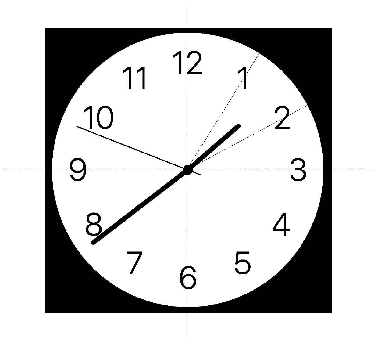
Technical field [0001] The present invention relates to the field of display technology, in particular to an AMOLED image processing method, driving chip and wearable equipment. Background technique [0002] The current mainstream display devices are generally liquid crystal display panels (LCD, Liquid Crystal Display) or active organic electroluminescence display panels (AMOLED, Active-Matrix Organic Light Emitting Diode). Compared with liquid crystal display panels, active organic electroluminescent display panels have the advantages of faster response speed, higher contrast, wider viewing angle, lower power consumption, and smaller module thickness. [0003] Moreover, the use of AMOLED in wearable products can be thinner and lighter in terms of shape specifications. Therefore, more and more wearable products currently use AMOLED as displays. However, wearable products, especially SmartWatch, most of the products have a circular display. When an array of pixels is used to displa...

Claims


Application Information

Patent Timeline
Patent Type & Authority Patents(China)
IPC IPC(8): G06F3/147G06F1/16
CPCG06F1/163G06F1/1637G06F3/147G09G2340/14G09G2320/0271G09G5/026G09G3/2003G09G3/2007G09G2310/0232G09G3/3208G06T5/002G06T5/20G06T2207/20021G06T2207/20192
Inventor 喻勇姚远兰传艳金兑炫
Owner BOE TECH GRP CO LTD
Learn More