Frameless display strip and screen splicing system
A display strip, borderless technology, applied in the direction of instruments, electrical components, electrical solid devices, etc., can solve the problems of screen splicing system split screen frame and other problems, and achieve the effect of reducing cost and convenient installation.
- Summary
- Abstract
- Description
- Claims
- Application Information
AI Technical Summary
Problems solved by technology
Method used
Image
Examples
Embodiment 1
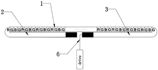
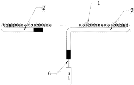
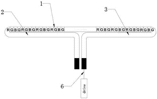
[0033] Such as figure 1As shown, the present invention provides a borderless display strip, the display panel material of the borderless display strip is flexible OLED; the OLED panel includes an effective display middle area 1 and two invalid display along the width direction Edge areas 2 and 3; edge area 2 does not contain lead circuits, and edge area 3 includes lead circuits 6; the aspect ratio of the borderless display bar is greater than 8, and the width of the borderless display bar refers to the effectively displayed The width of the middle area 1; the edge area 2 and the edge area 3 are bent and directly adhered to the back of the middle area, and the bending radius R is less than 1.3mm, such as Figure 4 As shown, the bending radius does not include the thickness of the OLED panel, and the bending radius R is preferably 0.1-0.4mm; the edge area 2 and the edge area 3 are all directly adhered to the back of the middle area 1 (such as figure 2 , image 3 As shown, the...
Embodiment 2
[0037] Such as Figure 11 As shown, the present invention provides a borderless display strip, the display panel material of the borderless display strip is flexible OLED; the OLED panel includes an effective display middle area 1 and two invalid display along the width direction Edge areas 2 and 3; edge area 2 does not contain lead circuits, and edge area 3 includes lead circuits 6; the aspect ratio of the borderless display bar is greater than 8, and the width of the borderless display bar refers to the effectively displayed The width of the middle region 1; the back side of the middle region 1 is adhered to the upper side of the multilayer flexible circuit 9, the edge region 2 and the edge region 3 are bent and adhered to the lower side of the multilayer flexible circuit 9, and the bending radius R is less than 1.3mm, such as Figure 4 As shown, the bending radius does not include the thickness of the OLED panel, and the bending radius 4 is preferably 0.2-0.5mm; the edge r...
PUM
 Abstract
Description
Claims
Application Information
 - R&D
- Intellectual Property
- Life Sciences
- Materials
- Tech Scout
- Unparalleled Data Quality
- Higher Quality Content
- 60% Fewer Hallucinations
Browse by: Latest US Patents, China's latest patents, Technical Efficacy Thesaurus, Application Domain, Technology Topic, Popular Technical Reports.
© 2025 PatSnap. All rights reserved.Legal|Privacy policy|Modern Slavery Act Transparency Statement|Sitemap|About US| Contact US: help@patsnap.com


