Detection device and detection method for array substrate row drive circuit
A technology of array substrate row and detection device, which is applied in power test, static indicator, instrument, etc., can solve the problem of increasing the difficulty of abnormal analysis, unable to further determine the abnormal row drive unit, etc., and shorten the investigation and repair time. , the effect of improving efficiency
- Summary
- Abstract
- Description
- Claims
- Application Information
AI Technical Summary
Problems solved by technology
Method used
Image
Examples
no. 1 example
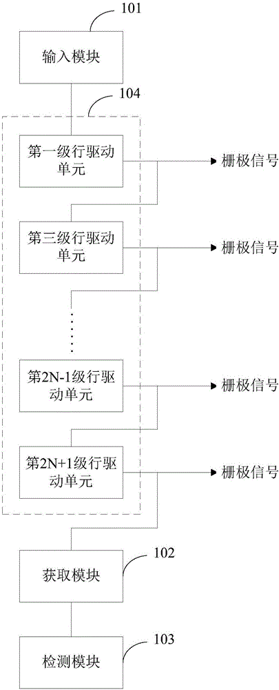
[0056] Generally speaking, the row driving circuit of the left array substrate and the row driving circuit of the right array substrate are detected separately. The detection method used is the same. Therefore, the detection of the row driving circuit of the left array substrate is taken as an example for description below.
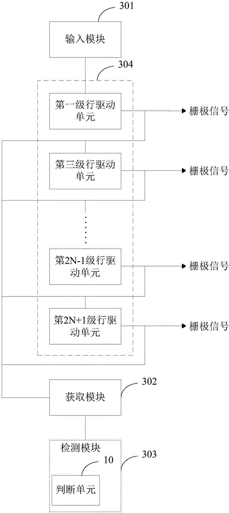
[0057] image 3 It is a schematic structural diagram of a detection device of the row driving circuit of the array substrate (here, the row driving circuit of the left array substrate, referred to as the row driving circuit) according to the first embodiment of the present invention. Such as image 3 As shown, the detection device mainly includes an input module 301 , an acquisition module 302 and a detection module 303 .
[0058] Specifically, the input module 301 is connected to the input terminal of the first-stage row driving unit of the row driving circuit 304 , and is used for inputting a test signal to the first-stage row driving unit of the row...
no. 2 example
[0067] This embodiment further optimizes the structure of the detection module 303 in the first embodiment.
[0068] Figure 4 is a schematic structural diagram of the detection module 303 according to the second embodiment of the present invention. Such as Figure 4 As shown, the detection module 303 of this embodiment may include a superposition unit 30 , a determination unit 40 and a plurality of conversion units 20 . Wherein, each conversion unit 20 is connected with the acquisition module 302 . And, each converting unit 20 corresponds to a row driving unit of one level, and is used for converting the output signal of the row driving unit of the level obtained by the acquisition module 302 into a pulse signal, and making the pulse signal correspond to the pulse of other row driving units. The signals do not overlap each other. The superposition unit 30 is respectively connected to each conversion unit 20, and is used for superimposing the pulse signals output by all co...
no. 3 example
[0078] Based on the same inventive concept, an embodiment of the present invention also provides a detection method for the array substrate row driving circuit 304 . Likewise, this embodiment still takes the row driving circuit 304 of the left array substrate as an example for illustration.
[0079] Figure 6 It is a schematic flowchart of the detection method of the array substrate row driving circuit 304 according to the third embodiment of the present invention. Such as Figure 6 As shown, the detection method may include the following steps S610, S620 and S630.
[0080] In step S610 , a test signal is input to the first-stage row driving unit of the row driving circuit 304 . Here, the row driving circuit 304 includes a plurality of cascaded row driving units.
[0081] In step S620, output signals of each row driving unit are acquired.
[0082] In step S630, when it is judged that the row driving circuit 304 is working abnormally, the abnormally working row driving uni...
PUM
 Abstract
Description
Claims
Application Information
 - R&D Engineer
- R&D Manager
- IP Professional
- Industry Leading Data Capabilities
- Powerful AI technology
- Patent DNA Extraction
Browse by: Latest US Patents, China's latest patents, Technical Efficacy Thesaurus, Application Domain, Technology Topic, Popular Technical Reports.
© 2024 PatSnap. All rights reserved.Legal|Privacy policy|Modern Slavery Act Transparency Statement|Sitemap|About US| Contact US: help@patsnap.com


