Solid state imaging device, ad converter and electronic equipment

A technology of solid-state imaging devices and converters, applied in AD converters, electronic equipment, and solid-state imaging devices, can solve problems such as crosstalk and achieve the effect of improving crosstalk characteristics

Active Publication Date: 2021-05-14
SONY CORP
View PDF10 Cites 0 Cited by
  • Summary
  • Abstract
  • Description
  • Claims
  • Application Information

AI Technical Summary

Problems solved by technology

This will cause crosstalk between adjacent pixels or adjacent AD converters

Method used


Image

  • Solid state imaging device, ad converter and electronic equipment
  • Solid state imaging device, ad converter and electronic equipment
  • Solid state imaging device, ad converter and electronic equipment

Examples


Embodiment Construction

[0026] Hereinafter, specific embodiments of the present invention will be described in detail with reference to the accompanying drawings.

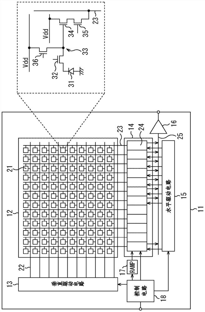
[0027] figure 1 is a block diagram showing a configuration example of an embodiment of the solid-state imaging device of the present invention.

[0028] exist figure 1 Among them, the solid-state imaging device 11 includes a pixel region 12 , a vertical drive circuit 13 , a column signal processing circuit 14 , a horizontal drive circuit 15 , an output circuit 16 , a ramp signal generation circuit (RAMP) 17 and a control circuit 18 .

[0029] A plurality of pixels 21 are arranged in an array in the pixel area 12 . Each pixel 21 is connected to the vertical drive circuit 13 via a horizontal signal line 22 , and is connected to the column signal processing circuit 14 via a vertical signal line 23 . Each of the plurality of pixels 21 outputs a pixel signal corresponding to the amount of light irradiated via an optical system (not shown). ...


PUM


Abstract

The present invention relates to a solid-state imaging device, an AD converter, and electronic equipment that can improve crosstalk characteristics. The AD converter has: a comparator for comparing a pixel signal and a reference signal; a pixel signal side capacitor connected between a pixel signal signal line for transmitting the pixel signal and one input terminal of the comparator; and a reference signal signal line for transmitting the reference signal. line to the reference signal side capacitor between the other input terminal of the comparator. The pixel signal side capacitor and the reference signal side capacitor are formed in such a manner that a second voltage generated between the comparator side node of the reference signal side capacitor and the pixel signal line side node of the pixel signal side capacitor connected to other adjacent AD converters is formed. A capacitor and a second capacitor generated between the comparator side node of the pixel signal side capacitor and the pixel signal line side node of the pixel signal side capacitor connected to adjacent other AD converters are substantially the same. The present invention is applicable to, for example, CMOS image sensors.

Description

technical field [0001] The present invention relates to a solid-state imaging device, an AD converter, and electronic equipment, and particularly to a solid-state imaging device, an AD converter, and electronic equipment for improving crosstalk characteristics. Background technique [0002] In related art electronic devices having imaging functions such as digital still cameras and digital video cameras, solid-state imaging devices such as charge coupled device (CCD) image sensors and complementary metal oxide semiconductor (CMOS) image sensors are used. A plurality of transistors and a photodiode (PD) for photoelectric conversion are combined in a pixel of a solid-state imaging device, and an image is constructed based on pixel signals output from a plurality of pixels arranged planarly. Furthermore, pixel signals output from the pixels are AD-converted by a plurality of AD (Analog to Digital) converters provided for each column of pixels, and the pixel signals are output. ...

Claims


Application Information

Patent Timeline
Patent Type & Authority Patents(China)
IPC IPC(8): H01L27/146H04N5/357H04N5/374
CPCH01L27/14643H04N25/617H04N25/76H04N25/75H04N25/65H01L27/14605H01L27/14636
Inventor 池田裕介穴井大二郎吉川玲
Owner SONY CORP
Why Eureka
Try Eureka