High-efficiency silicon wafer degumming device

A silicon wafer degumming and high-efficiency technology, applied in electrical components, semiconductor/solid-state device manufacturing, circuits, etc., can solve the problems of residue, unfavorable cleaning, unsatisfactory degumming effect, etc., to protect safety, improve utilization, and improve degumming effect. Effect

Inactive Publication Date: 2017-03-22
浙江傲尔科技有限公司
View PDF5 Cites 2 Cited by
  • Summary
  • Abstract
  • Description
  • Claims
  • Application Information

AI Technical Summary

Problems solved by technology

The degumming effect of the existing degumming device is not ideal, and it is easy to produce a large amount of residue after degumming is completed, which is not conducive to subsequent cleaning

Method used


Image

  • High-efficiency silicon wafer degumming device
  • High-efficiency silicon wafer degumming device
  • High-efficiency silicon wafer degumming device

Examples


Embodiment Construction

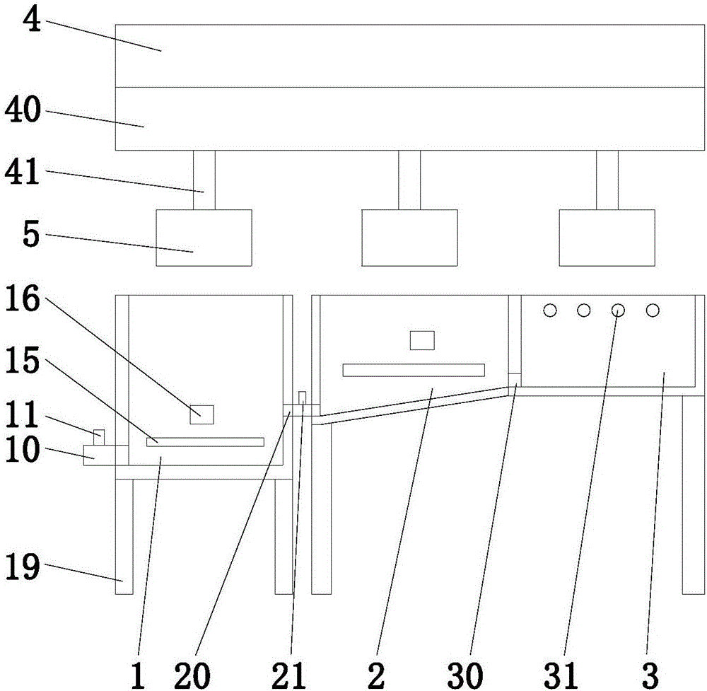
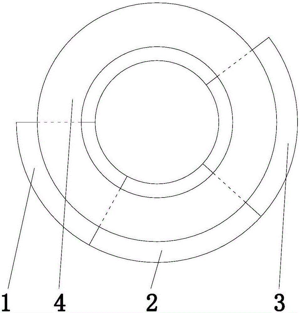
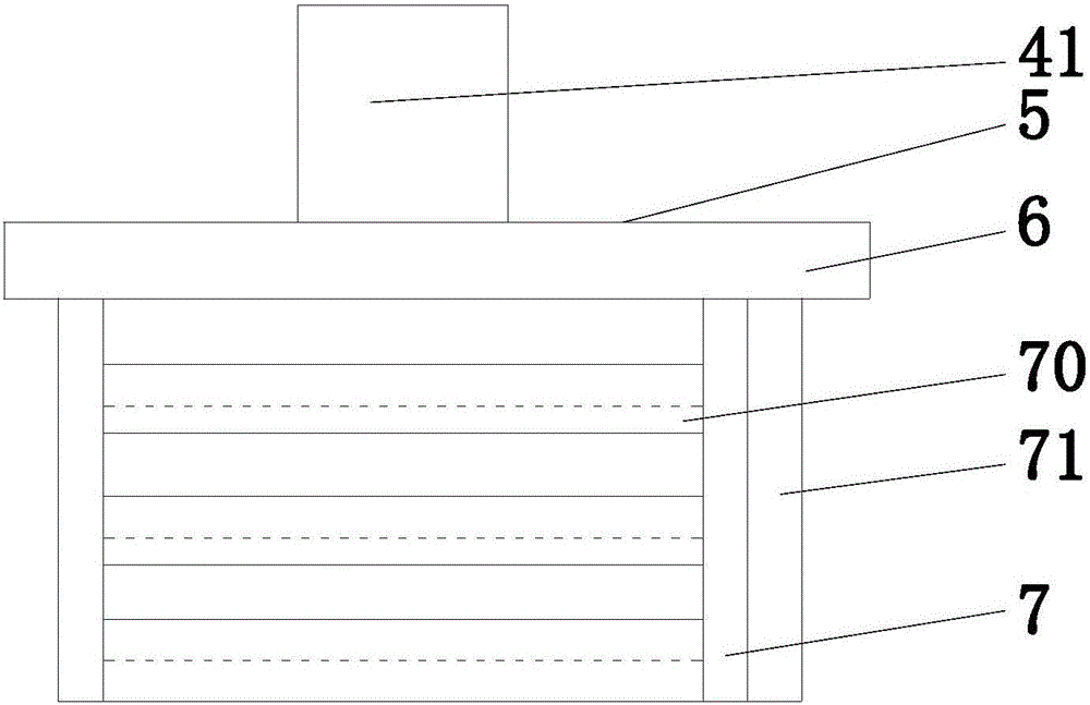
[0023] refer to figure 1 , figure 2 , image 3 and Figure 4 , a high-efficiency silicon wafer degumming device of the present invention comprises a fixed ring frame 4, a movable ring frame 40, a degumming support 5, a first degumming tank 1, a second degumming tank 2, and a filtrate tank 3. The fixed ring frame 4. A rotatable movable ring frame 40 is installed at the bottom, and 5 mutually independent telescopic rods 41 are installed on the bottom of the movable ring frame 40. The bottom of the telescopic rods 41 is fixed with a degumming support 5, and the degumming support 5 consists of a top plate 6, a vertical Composed of upright columns 7, U-shaped frames 70, and baffle plates 71, four vertical columns 7 are fixed on the bottom of the top plate 6, and the four vertical columns 7 form a rectangular array. A number of horizontally arranged U-shaped frames 70 are fixed up and down. The cross-section of the U-shaped frames 70 is L-shaped, and the opening ends of all U-sh...


PUM


Abstract

The invention discloses a high-efficiency silicon wafer degumming device. The high-efficiency silicon wafer degumming device comprises a fixed annular rack, a movable annular rack, a degumming support, a first degumming groove, a second degumming groove and a filtration groove, wherein the movable annular rack which can rotate is arranged at the bottom of the fixed annular rack, five telescopic rods which are independent to one another are arranged at the bottom of the movable annular rack, the degumming support is fixedly arranged at the bottoms of the telescopic rods and comprises a top plate, vertical posts, U-shaped frames and a baffle plate, and the first degumming groove, the second degumming groove and the filtration groove are arranged under the movable annular rack. The degumming support is connected with the movable annular rack by the telescopic rods, so that the degumming support can automatically pass through the first degumming groove, the second degumming groove and the filtration groove, the degumming device is convenient to use, and the degumming efficiency is improved.

Description

[0001] 【Technical field】 [0002] The invention relates to the technical field of polysilicon production, in particular to the technical field of silicon wafer degumming tanks. [0003] 【Background technique】 [0004] The cleanliness of the silicon wafer surface is a key factor affecting the silicon wafer yield and cell conversion efficiency. In order to obtain silicon wafers with high cleanliness, silicon wafers often need degumming cleaning and fine cleaning after wire cutting. The degumming effect of the existing degumming device is not ideal, and a large amount of residue is likely to be generated after the degumming is completed, which is not conducive to subsequent cleaning. [0005] 【Content of invention】 [0006] The object of the present invention is to solve the problems in the prior art, and propose a high-efficiency silicon wafer degumming device, which can improve the degumming effect of silicon wafers and improve the degumming efficiency at the same time. [00...

Claims


Application Information

Patent Timeline
Patent Type & Authority Applications(China)
IPC IPC(8): H01L21/67
CPCH01L21/67057H01L21/67034
Inventor 凌晓国岳旭余传江
Owner 浙江傲尔科技有限公司
Why Eureka
Try Eureka