Method for optimizing wafer edge defects of CMOS image sensor
An image sensor and edge defect technology, applied in the direction of electric solid-state devices, semiconductor devices, electrical components, etc., can solve the problems of bombarding silicon oxide, failure to grow silicon nitride, and affecting yield
- Summary
- Abstract
- Description
- Claims
- Application Information
AI Technical Summary
Problems solved by technology
Method used
Image
Examples
Embodiment Construction
[0028] In order to make the content of the present invention clearer and easier to understand, the content of the present invention will be described in detail below in conjunction with specific embodiments and accompanying drawings.
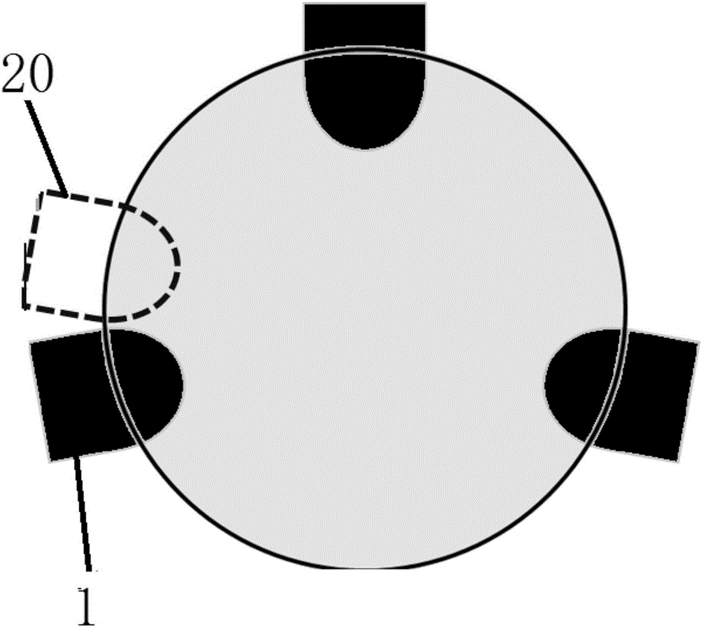
[0029] The present invention adjusts the different angles of different wafers located in the etching chamber in multiple steps, and gradually removes the low-temperature silicon dioxide (LTO) material dropped during the etching process on the back of the CIS wafer, so that the etching chamber is independently generated from the defect source To the function of self-clearing, thereby greatly reducing online defects and improving product yield.
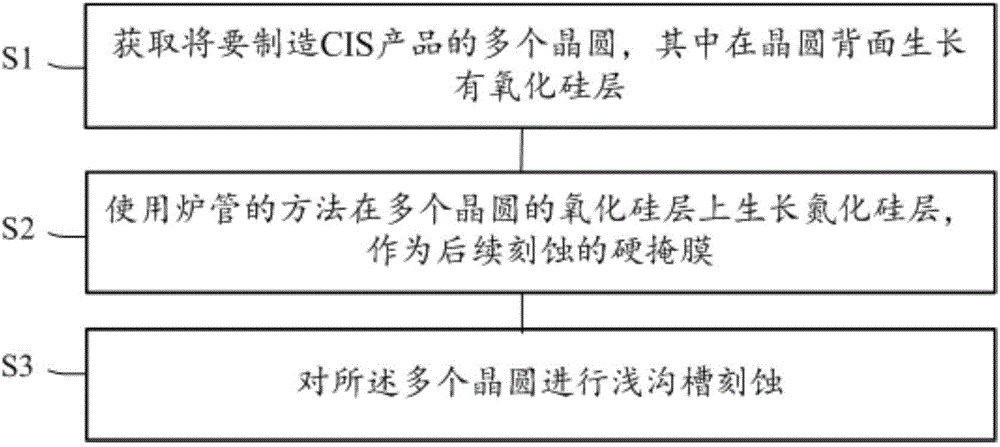
[0030] figure 2 A flow chart of a method for optimizing edge defects of a CMOS image sensor wafer according to a preferred embodiment of the present invention is schematically shown.
[0031] Such as figure 2 As shown, the method for optimizing CMOS image sensor wafer edge defects according to a prefe...
PUM
 Abstract
Description
Claims
Application Information
 - Generate Ideas
- Intellectual Property
- Life Sciences
- Materials
- Tech Scout
- Unparalleled Data Quality
- Higher Quality Content
- 60% Fewer Hallucinations
Browse by: Latest US Patents, China's latest patents, Technical Efficacy Thesaurus, Application Domain, Technology Topic, Popular Technical Reports.
© 2025 PatSnap. All rights reserved.Legal|Privacy policy|Modern Slavery Act Transparency Statement|Sitemap|About US| Contact US: help@patsnap.com


