Display device, liquid crystal display and method of eliminating ghost
A liquid crystal display and a technology for a display device are applied in the field of display devices, liquid crystal displays and the elimination of afterimages, which can solve problems such as afterimages of liquid crystal display modules, and achieve the effects of improving reliability and eliminating afterimages.
- Summary
- Abstract
- Description
- Claims
- Application Information
AI Technical Summary
Problems solved by technology
Method used
Image
Examples
Embodiment 1
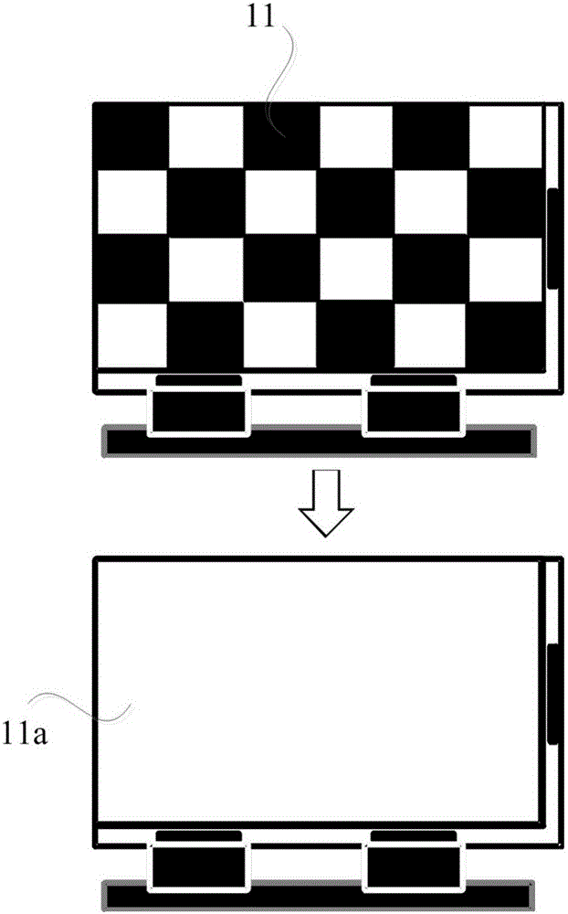
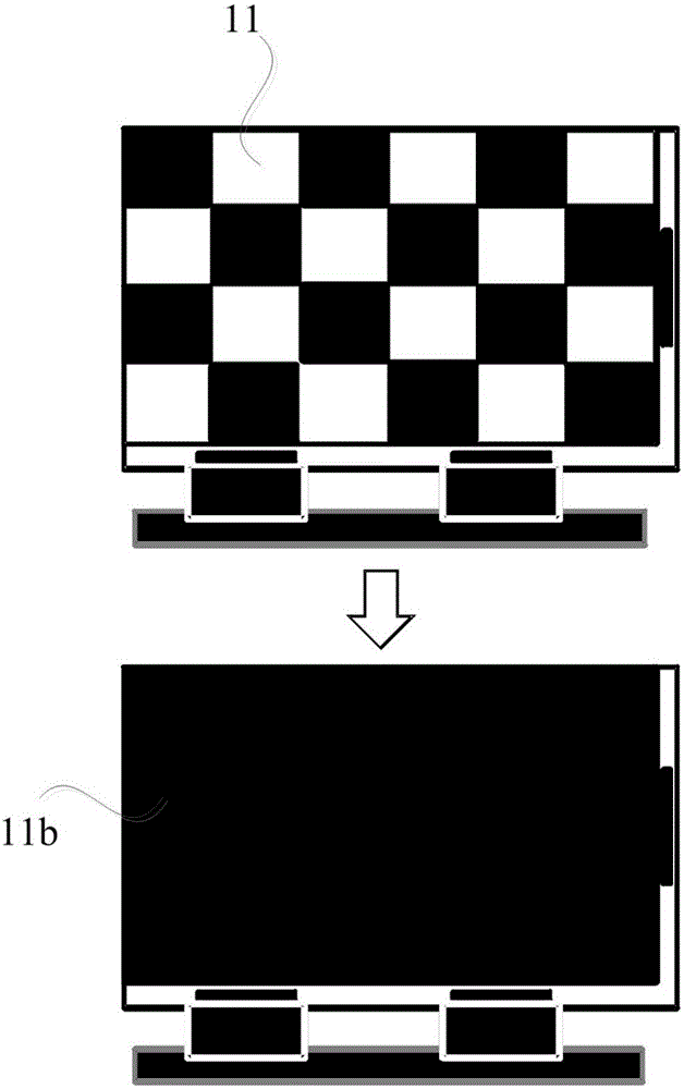
[0060] Please refer to figure 1 , figure 1 It is a schematic structural diagram of a display device provided in Embodiment 1 of the present invention. like figure 1 As shown, the display device includes a display module 11 , a data driver 12 , a power module 13 and a timing controller 14 .
[0061] In this embodiment, the display module 11 includes several pixel units arranged in an array, wherein each pixel unit may include a thin film transistor, a storage capacitor, a driving chip and a switching element. Those skilled in the art may combine the Each element of the above-mentioned pixel unit is used to realize the normal operation of the pixel unit. Of course, designers can also design pixel units according to job requirements. The display module 11 may be a twisted nematic display module (Twisted Nematic, TN) or a multi-domain vertical alignment display module (Multi-domain Vertical Alignment, MVA) or a transverse electric field display module (In-Plain Switching, IPS)...
Embodiment 2
[0069] Please refer to figure 2 , figure 2 It is a schematic structural diagram of a display device provided in Embodiment 2 of the present invention. like figure 2 As shown, the display device includes a display module 21 , a data driver 22 , a power module 23 , a timing controller 24 and a gate driver 25 .
[0070] In this embodiment, the display module 21 includes several pixel units arranged in an array, wherein each pixel unit may include a thin film transistor, a storage capacitor, a driving chip and a switching element. Those skilled in the art may combine Each element of the above-mentioned pixel unit is used to realize the normal operation of the pixel unit. Of course, designers can also design pixel units according to job requirements. The display module 21 may be a twisted nematic display module (Twisted Nematic, TN) or a multi-domain vertical alignment display module (Multi-domain Vertical Alignment, MVA) or a transverse electric field display module (In-Pla...
Embodiment 3
[0076] Please refer to image 3 , image 3 It is a schematic structural diagram of a display device provided in Embodiment 3 of the present invention. like image 3 As shown, the display device includes a display module 31 , a data driver 32 , a power module 33 , a timing controller 34 , a gate driver 35 and a backlight 36 .
[0077] In this embodiment, the display module 31 includes several pixel units arranged in an array, wherein each pixel unit may include a thin film transistor, a storage capacitor, a driving chip and a switching element. Those skilled in the art may combine Each element of the above-mentioned pixel unit is used to realize the normal operation of the pixel unit. Of course, designers can also design pixel units according to job requirements. The display module 31 may be a twisted nematic display module (Twisted Nematic, TN) or a multi-domain vertical alignment display module (Multi-domain Vertical Alignment, MVA) or a transverse electric field display ...
PUM
 Abstract
Description
Claims
Application Information
 - R&D
- Intellectual Property
- Life Sciences
- Materials
- Tech Scout
- Unparalleled Data Quality
- Higher Quality Content
- 60% Fewer Hallucinations
Browse by: Latest US Patents, China's latest patents, Technical Efficacy Thesaurus, Application Domain, Technology Topic, Popular Technical Reports.
© 2025 PatSnap. All rights reserved.Legal|Privacy policy|Modern Slavery Act Transparency Statement|Sitemap|About US| Contact US: help@patsnap.com


