A method for constructing nonlinear scalable models of gan high electron mobility transistors
A high electron mobility and transistor technology, applied in the field of microelectronics, can solve the problems of model inaccuracy, incompatibility, tedious time-consuming, etc., and achieve the effect of reducing optimization steps, avoiding tedious steps, and reducing dependence
- Summary
- Abstract
- Description
- Claims
- Application Information
AI Technical Summary
Problems solved by technology
Method used
Image
Examples
Embodiment Construction
[0032] specific implementation plan
[0033] The principles and features of the present invention are described below in conjunction with the accompanying drawings, and the examples given are only used to explain the present invention, and are not intended to limit the scope of the present invention.
[0034] In this example, AlGaN / GaN high electron mobility transistor HEMT device is taken as an example to establish a nonlinear scalable model of GaN HEMT.
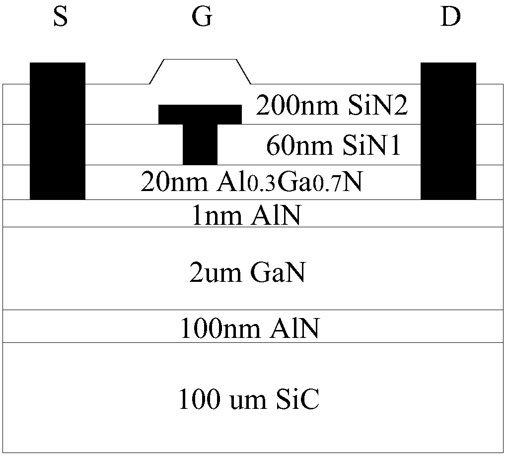
[0035] refer to figure 1 , an AlGaN / GaN high electron mobility transistor HEMT device, which includes a 2-inch 4H-SiC substrate, a 100nm thick AlN nucleation layer, a 2um thick GaN buffer layer, a 1nm AlN insertion layer, and a 20nm thick non- Doped AlGaN barrier layer, 60nm SiN passivation layer, Ti / Al / Ni / Au ohmic source electrode and ohmic drain electrode, Ni / Au / Ni Schottky gate, where the gate width is 10×100um, and the gate length is 0.25um, gate-gate, gate-source, gate-drain pitches are 40um, 0.7um and 2.8um respecti...
PUM
 Abstract
Description
Claims
Application Information
 - R&D
- Intellectual Property
- Life Sciences
- Materials
- Tech Scout
- Unparalleled Data Quality
- Higher Quality Content
- 60% Fewer Hallucinations
Browse by: Latest US Patents, China's latest patents, Technical Efficacy Thesaurus, Application Domain, Technology Topic, Popular Technical Reports.
© 2025 PatSnap. All rights reserved.Legal|Privacy policy|Modern Slavery Act Transparency Statement|Sitemap|About US| Contact US: help@patsnap.com


