High aspect ratio structure

A high aspect ratio structure and support structure technology, applied in electrical components, electrical solid devices, circuits, etc., can solve the problems of poor electrical testing of semiconductor components, difficult process connection, structural bending, etc., to improve strength and collapse resistance. , avoid bending or collapsing, overcome the effect of bending or collapsing

Inactive Publication Date: 2016-06-22
MACRONIX INT CO LTD
View PDF3 Cites 0 Cited by
  • Summary
  • Abstract
  • Description
  • Claims
  • Application Information

AI Technical Summary

Problems solved by technology

For example, when forming a high aspect ratio (higher aspect ratio, HAR) structure, such as a trench with a high aspect ratio, the challenge to be faced is that the structures on both sides of the trench are prone to bending or collapse
This phenomenon not only causes difficulties in the connection of subsequent processes, but also causes adverse effects on the electrical testing of semiconductor components.

Method used


Image

  • High aspect ratio structure
  • High aspect ratio structure
  • High aspect ratio structure

Examples


Embodiment Construction

[0047] In order to further explain the technical means and effects of the present invention to achieve the intended purpose of the invention, the specific implementation, structure, characteristics and effects of the high aspect ratio structure proposed according to the present invention will be described below in conjunction with the accompanying drawings and preferred embodiments. , as detailed below.

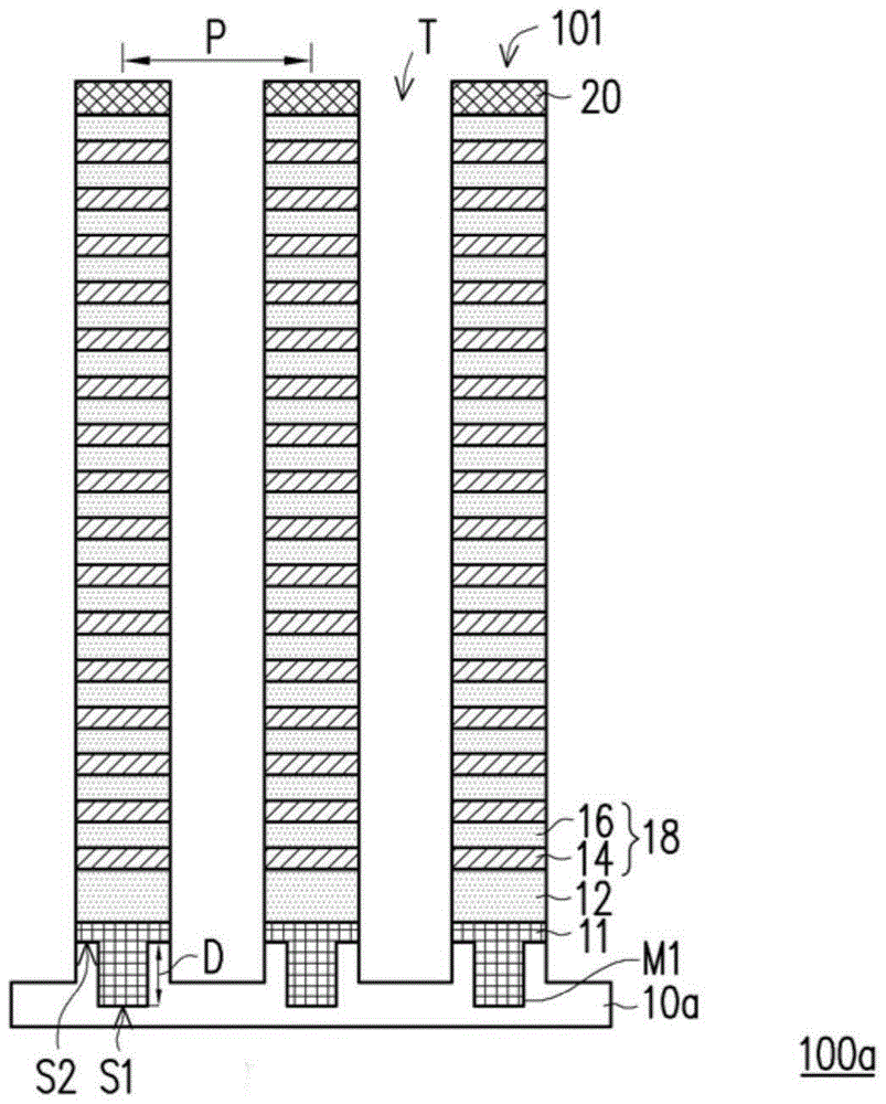
[0048] Figure 1A is a schematic cross-sectional view of a high aspect ratio structure according to an embodiment of the present invention.

[0049] see Figure 1A As shown, the high aspect ratio structure 100 a includes a substrate 10 a , a plurality of stacked structures 101 and a plurality of support structures 11 . The substrate 10a may comprise a semiconductor material, an insulator material, a conductive material, or any combination thereof. The material of the substrate 10a is, for example, selected from Si, SiO 2 , Ge, SiGe, GaP, GaAs, SiC, SiGeC, InAs and InP in th...


PUM


Abstract

A high aspect ratio structure is provided. The high aspect ratio structure includes a substrate, a plurality of stack structures, and a plurality of support structures. The stack structures are disposed on the substrate, and a trench is formed between adjacent two stack structures. Each of the stack structures includes a plurality of first material layers and a plurality of second material layers. The second material layers and the first material layers are disposed alternately. The support structures are respectively disposed between the substrate and the stack structures, wherein each of the support structures has a concave-convex surface.

Description

technical field [0001] The present invention relates to a high aspect ratio structure. Background technique [0002] As the size of semiconductor devices shrinks, in order to achieve high density and high performance, the manufacturing method of semiconductor devices has also evolved into stacking vertically upwards to more effectively utilize the wafer area. [0003] In the vertical memory device, when the device structure is stacked upwards, the relative relationship between each device and the structure of the stacked structure also become complicated. For example, when forming a high aspect ratio (high aspect ratio, HAR) structure, such as a trench with a high aspect ratio, the challenge is that the structures on both sides of the trench are likely to bend or collapse. This phenomenon not only causes difficulties in the connection of the subsequent process, but also causes adverse effects on the electrical testing of the semiconductor element. Therefore, how to avoid b...

Claims


Application Information

Patent Timeline
Patent Type & Authority Applications(China)
IPC IPC(8): H01L27/115H01L29/06
CPCH01L2924/0002H10B41/35H10B41/27H10B43/35H10B43/27H01L2924/00
Inventor 张升原魏安祺连楠梓杨大弘陈光钊
Owner MACRONIX INT CO LTD
Why Eureka
Try Eureka