Colored film base plate and manufacturing method thereof, liquid crystal display panel and display device
A color filter substrate and display area technology, applied in nonlinear optics, instruments, optics, etc., can solve the problems of poor display effect and low uniformity of liquid crystal display panels, and achieve improved uniformity, improved display uniformity, and increased height. Effect
- Summary
- Abstract
- Description
- Claims
- Application Information
AI Technical Summary
Problems solved by technology
Method used
Image
Examples
Embodiment 1
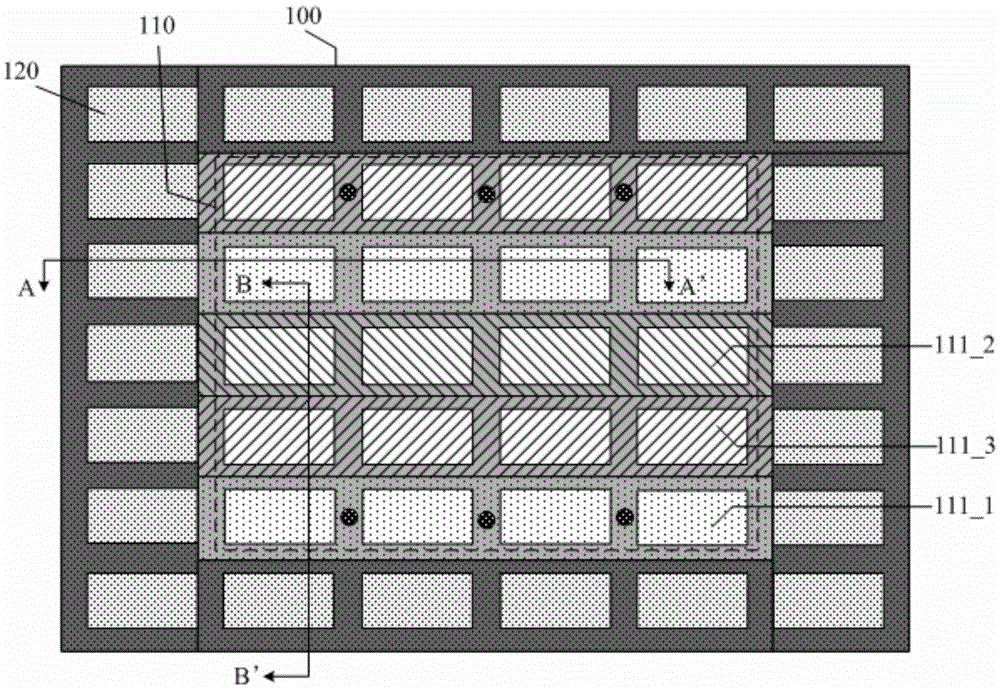
[0035] An embodiment of the present invention provides a color filter substrate, such as image 3 As shown, it includes: a base substrate 100, a black matrix located on the base substrate 100 ( image 3 have been blocked), the base substrate 100 is divided into a display area 110 and a peripheral area surrounding the display area 110; wherein, the display area 110 is provided with a plurality of colors of the first photoresist layer 111_n (n=1, 2, 3...N; wherein N is the number of different colors in the first photoresist layer; image 3 Take N equal to 3 as an example),
[0036] The structure of the black matrix in the display area 110 and the surrounding area is the same;
[0037] The color filter substrate also includes: a light-shielding portion 120 located in the peripheral area and covering at least the base substrate 100; wherein the light-shielding portion 120 includes at least two second photoresist layers ( image 3 not shown).
[0038] The above-mentioned color ...
Embodiment 2
[0048] For example, if Figure 4b As shown, the material of the second photoresist layer 121_1 is the same as that of the blue first photoresist layer 111_1 ; the material of the second photoresist layer 121_2 is the same as that of the red first photoresist layer 111_2 . Can form the pattern of the blue first photoresist layer and the pattern of the second photoresist layer simultaneously by one patterning process like this, and simultaneously form the pattern of the first photoresist layer of red and the pattern of the second photoresist layer, can simplify craft.
Embodiment 3
[0050] Of course, in actual implementation, in order to improve the light-shielding effect of the light-shielding portion, the number of second photoresist layers in the light-shielding portion can be increased. For example, if Figure 5b As shown (taking N equal to 3 as an example), the material of the second photoresist layer 121_1 is the same as that of the blue first photoresist layer 111_1; the material of the second photoresist layer 121_2 is the same as that of the red first photoresist layer 111_2; The material of the photoresist layer 121_3 is the same as that of the green first photoresist layer 111_3 .
[0051] Specifically, generally the transmittance of the blue first photoresist layer and the red first photoresist layer is lower than the transmittance of the green first photoresist layer, that is, the blue first photoresist layer and the red first photoresist layer The light-shielding performance of the green first photoresist layer is better than that of the gr...
PUM
 Abstract
Description
Claims
Application Information
 - R&D
- Intellectual Property
- Life Sciences
- Materials
- Tech Scout
- Unparalleled Data Quality
- Higher Quality Content
- 60% Fewer Hallucinations
Browse by: Latest US Patents, China's latest patents, Technical Efficacy Thesaurus, Application Domain, Technology Topic, Popular Technical Reports.
© 2025 PatSnap. All rights reserved.Legal|Privacy policy|Modern Slavery Act Transparency Statement|Sitemap|About US| Contact US: help@patsnap.com


