Circuit board manufacturing method and circuit board

A circuit board manufacturing and circuit board technology, which is applied in the directions of printed circuit components, electrical connection printed components, and electrical connection formation of printed components, etc. , to achieve the effect of improving quality, reducing risk, and reducing the possibility of separation

Active Publication Date: 2016-04-06
SHENNAN CIRCUITS
View PDF4 Cites 4 Cited by
  • Summary
  • Abstract
  • Description
  • Claims
  • Application Information

AI Technical Summary

Problems solved by technology

[0004] However, buried lines will be affected by etching such as differential etching and super-roughening, which will cause the surface of the line to be lower than the surface of the substrate. Due to the height difference between the surface of the line and the substrate, the bonding force between the line and the substrate will also be affected. , especially the sidewall of the circuit and the substrate resin are prone to separation, so this defect will directly affect the quality of the product and cause reliability risks

Method used


Image

  • Circuit board manufacturing method and circuit board
  • Circuit board manufacturing method and circuit board
  • Circuit board manufacturing method and circuit board

Examples


Embodiment Construction

[0041] The following will clearly and completely describe the technical solutions in the embodiments of the present invention with reference to the accompanying drawings in the embodiments of the present invention. Obviously, the described embodiments are only some, not all, embodiments of the present invention. Based on the embodiments of the present invention, all other embodiments obtained by those skilled in the art without creative efforts fall within the protection scope of the present invention.

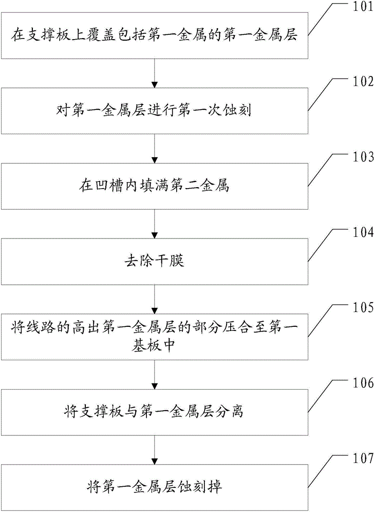
[0042] see figure 1 , an embodiment of a method for manufacturing a circuit board in an embodiment of the present invention includes:

[0043] 101. Cover the support plate with a first metal layer including a first metal;

[0044] A support plate is prepared, and the support plate is covered with a first metal layer including a first metal.

[0045] 102. Etching the first metal layer for the first time;

[0046] After the first metal layer is covered on the support plate, a...


PUM


Abstract

The embodiment of the invention discloses a circuit board manufacturing method for reducing the possibility of the separation of the side wall of a line and a base resin, and thus the effect of improving the quality of a product is achieved. The method of the embodiment of the invention comprises a step of covering a first metal layer with a first metal on a support plate, a step of carrying out first time of etching on the first metal layer through covering a developed dry film on the first metal layer such that a groove is formed on the first metal layer, a step of filling the groove with a second metal which forms the line, a step of removing the dry film such that the line has a part which is higher than the first metal layer, a step of pressing the part of the line which is higher than the first metal layer into the first substrate, and a step of separating the support plate and the first metal layer and carrying second time of etching on the first metal layer so as to remove the first metal layer. The embodiment of the invention discloses a circuit board, and the quality of the product can be improved.

Description

technical field [0001] The invention relates to the field of circuit board production, in particular to a circuit board production method and a circuit board. Background technique [0002] Printed circuit board (English: PrintedCircuitBoard, referred to as PCB), the role of PCB in electronic devices and system technology is becoming more and more important. And volume development, the PCB as a device and system connection role is also developing towards a high-density PCB with miniaturized connections. With the continuous increase in the heat density of electronic products, the demand for PCB circuit design is also receiving more and more attention. [0003] In the prior art, the embedding design scheme is adopted to embed the circuits on the circuit board into the substrate, which can eliminate the influence of side etching on the line width and line spacing during the manufacturing process, thereby improving the density and precision of wiring. High-density packaging is a...

Claims


Application Information

Patent Timeline
Patent Type & Authority Applications(China)
IPC IPC(8): H05K1/11H05K3/40
Inventor 李飒熊佳谷新
Owner SHENNAN CIRCUITS
Why Eureka
Try Eureka