


Quick Research
Generate reliable direction feasibility study reports for your R&D in just a few steps.

Technical Q&A
Discover and master advanced knowledge NOW. Basics, ideas, possibilities, all at once.

Find Solutions
As an expert in R&D theories, this can generate solutions to your technical problems instantly.

Evaluate Feasibility
Analyze your overall solution with one click, know your potential R&D risks in advance.

Monitor Landscape
Get weekly tech updates, stay abreast of the latest tech innovations and key insights.
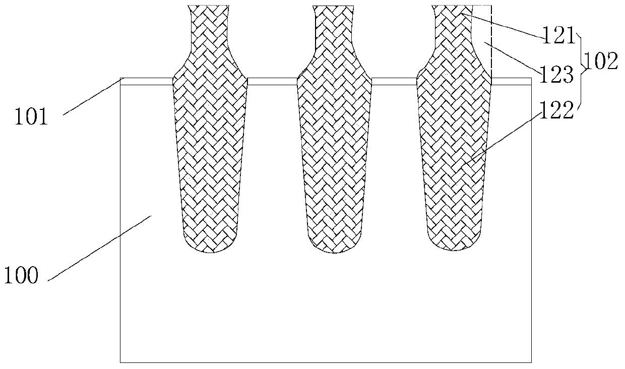
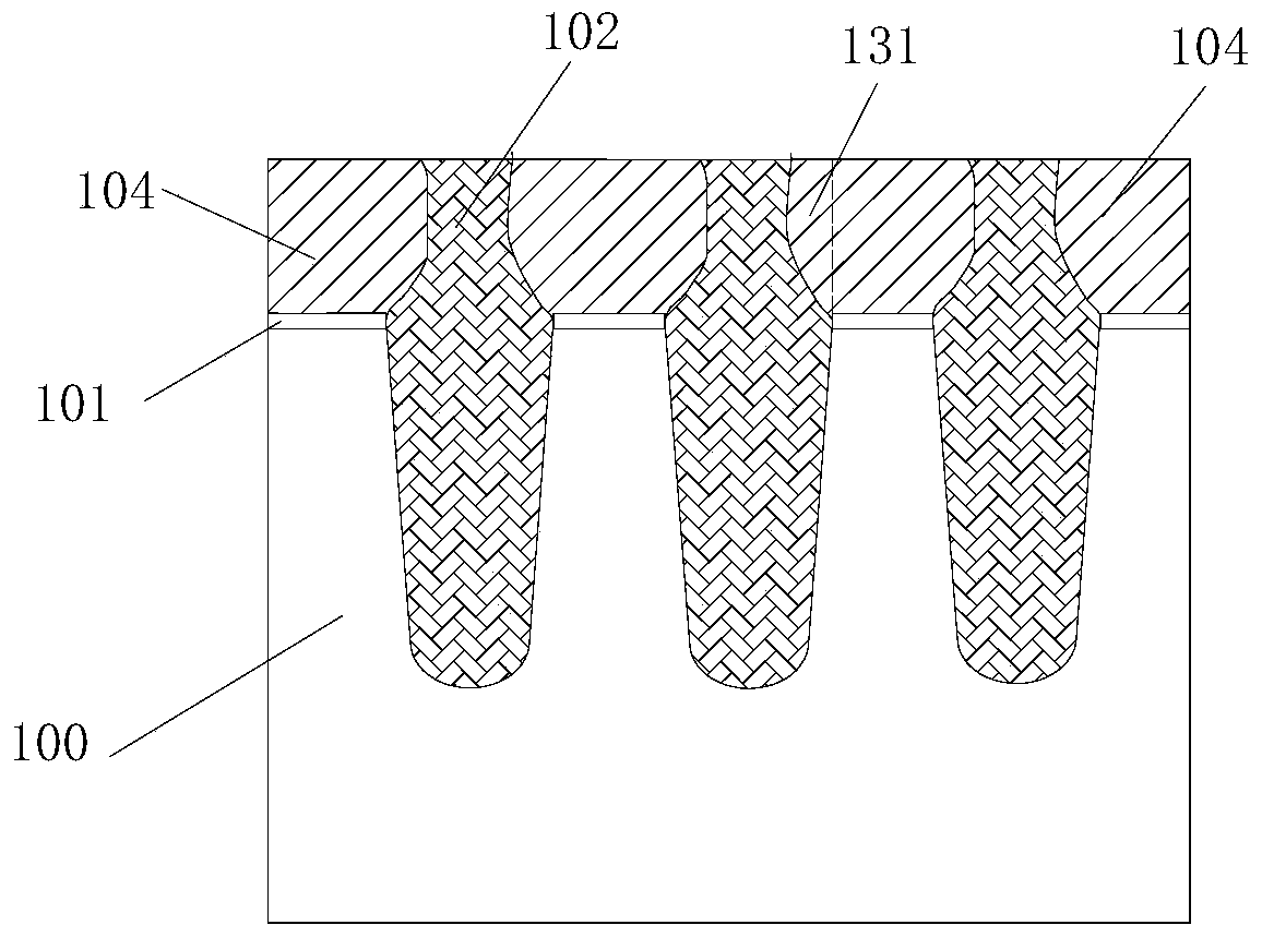
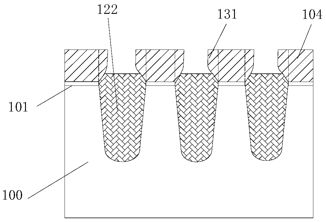
A method of manufacturing a floating grid
A manufacturing method and technology of floating gates, which are applied in the direction of semiconductor devices, etc., and can solve the problems of mutual interference of floating gates 104, data loss of storage devices, irregular shapes of floating gates 104, etc.
- Summary
- Abstract
- Description
- Claims
- Application Information
AI Technical Summary
Problems solved by technology
Method used
Image

Examples
Embodiment Construction
[0036] It should be pointed out that the following detailed description is exemplary and intended to provide further explanation to the present application. Unless defined otherwise, all technical and scientific terms used herein have the same meaning as commonly understood by one of ordinary skill in the art to which this application belongs.
[0037] It should be noted that the terminology used here is only for describing specific implementations, and is not intended to limit the exemplary implementations according to the present application. As used herein, unless the context clearly indicates otherwise, the singular form is also intended to include the plural form. In addition, it should also be understood that when the terms "comprising" and / or "comprising" are used in this specification, it indicates There are features, steps, operations, means, components and / or combinations thereof.
[0038] For the convenience of description, spatially relative terms may be used here...
PUM
 Abstract
Description
Claims
Application Information
 - R&D Engineer
- R&D Manager
- IP Professional
- Industry Leading Data Capabilities
- Powerful AI technology
- Patent DNA Extraction
Browse by: Latest US Patents, China's latest patents, Technical Efficacy Thesaurus, Application Domain, Technology Topic, Popular Technical Reports.
© 2024 PatSnap. All rights reserved.Legal|Privacy policy|Modern Slavery Act Transparency Statement|Sitemap|About US| Contact US: help@patsnap.com