Organic light emitting display and manufacture method thereof

A technology of a light-emitting display and a manufacturing method, which are applied in the directions of organic semiconductor devices, semiconductor/solid-state device manufacturing, and electric solid-state devices, etc., to achieve the effect of smooth output current

Active Publication Date: 2015-12-16
TCL CHINA STAR OPTOELECTRONICS TECH CO LTD +1
View PDF3 Cites 4 Cited by
  • Summary
  • Abstract
  • Description
  • Claims
  • Application Information

AI Technical Summary

Problems solved by technology

However, in the existing manufacturing technology, the TFT manufactured by the manufacturing method cannot meet the above requirements

Method used


Image

  • Organic light emitting display and manufacture method thereof
  • Organic light emitting display and manufacture method thereof
  • Organic light emitting display and manufacture method thereof

Examples


Embodiment Construction

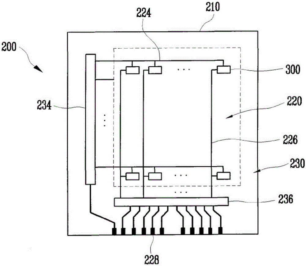
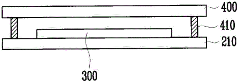
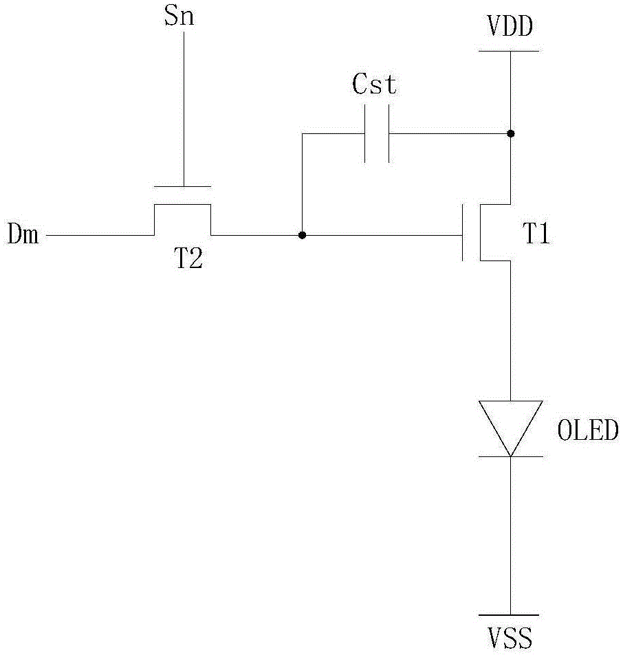
[0024] Hereinafter, embodiments of the present invention will be described in detail with reference to the accompanying drawings. This invention may, however, be embodied in many different forms and should not be construed as limited to the specific embodiments set forth herein. Rather, the embodiments are provided to explain the principles of the invention and its practical application, thereby enabling others skilled in the art to understand the invention for various embodiments and with various modifications as are suited to particular intended uses. In the drawings, the thicknesses of layers and regions are exaggerated for clarity of devices, and the same reference numerals will be used to refer to the same elements throughout the specification and drawings. It will also be understood that when a layer or element is referred to as being "on" another layer or substrate, it can be directly on the other layer or substrate, or intervening layers may also be present.

[0025] ...


PUM


Abstract

The invention discloses an organic light emitting display and a manufacture method thereof. The manufacture method comprises that a grid (20) of a first thin film transistor (T1) is formed on a substrate (10); a first insulated combination layer (12) which covers the grid (20), source and drain electrodes (22a and 22b) placed on the first insulated combination layer (12) of the first thin film transistor (T1), source and drain electrodes (32a and 32b) of a second thin film transistor (T2), a storage capacitor (Cst) and a first storage electrode (40) are continuously formed on the substrate (10); a third insulated layer (16) which covers the source electrode (22a), the drain electrode (22b), the source electrode (32a), the drain electrode (32b) and the first storage electrode (40) is formed on the first insulated combination layer (12); a grid (30) of the second thin film transistor (T2) and a second storage electrode (42) of the storage capacitor (Cst) are formed on the third insulated layer (16); a second insulated combination layer (18) which covers the grid (30) and the second storage electrode (42) is formed on the third insulated layer (16); and through holes (18') are formed in the second insulated combination layer (18) so that the source electrode (22a), the drain electrode (22b), the source electrode (32a) and the drain electrode (32b) are exposed.

Description

technical field [0001] The invention belongs to the field of display technology, and in particular relates to an organic light-emitting display and a manufacturing method thereof. Background technique [0002] Compared with a liquid crystal display (LCD), an organic light emitting display has self-luminescence characteristics and excellent display characteristics, such as viewing angle, contrast ratio, response speed, power consumption, and the like. [0003] An organic light emitting display may include an organic light emitting diode (OLED) having an anode, an organic thin film, and a cathode. Organic light emitting displays can be classified into passive matrix type or active matrix type. In passive matrix type organic light emitting display, OLEDs are connected to each other by a matrix method between scan lines and data lines to form pixels, while in active matrix type In OLEDs, individual pixels are controlled by thin-film transistors (TFTs) that act as switches. [...

Claims


Application Information

Patent Timeline
Patent Type & Authority Applications(China)
IPC IPC(8): H01L27/32H01L51/56
CPCH10K59/125H10K71/00H01L27/1251H01L27/1255H10K59/1216H10K59/1213H10K59/1201H10K2102/351H10K59/124
Inventor 汤富雄
Owner TCL CHINA STAR OPTOELECTRONICS TECH CO LTD
Why Eureka
Try Eureka