
Methods and devices for acquiring signals and tracking cells by adopting light sensitive chips

A photosensitive chip, a technology for collecting signals, applied in the field of information collection, can solve the problems of time difference, incomparability of signal strength, and reduced sensitivity, so as to achieve the effect of not reducing resolution, avoiding optical signal loss, and improving sensitivity

Inactive Publication Date: 2015-11-18
SANGHAI E BLOT PHOTOELECTRIC TECHNOLOGY CO LTD
View PDF6 Cites 4 Cited by
  • Summary
  • Abstract
  • Description
  • Claims
  • Application Information

AI Technical Summary

Problems solved by technology

There are the following disadvantages: 1. It takes up a lot of space: special darkrooms (rooms), sinks, and sewer pipes, etc. are required
2. High cost: Not only do you need to buy film processors and cassettes, but you also need a lot of consumables such as photosensitive film, developer, and fixer
Washing the film also causes waste of water resources
3. Pollution of the environment: developing film requires a lot of developer and fixer
4. Unstable image quality: In the darkroom, researchers cannot monitor the exposure level in real time, and often get a better image after several attempts
Time-consuming
5. Time-consuming: Nowadays, digitalization is widely used for data storage, transmission and publication. Therefore, film images have to be scanned and converted into digital images
6. Quantitative inaccuracy: Most of the time, the image that researchers judge to be better with the naked eye is actually oversaturated in grayscale
Disadvantage: loses the advantages of film acquisition, that is, the sensitivity is severely reduced
Disadvantages: Since the optical signal is collected by linear scanning, the entire image cannot be collected at the same time, so there is a time difference between scanning in different areas
And because the light source is continuously attenuated with time, the signal strength collected at different time points will not be comparable
Makes many controlled trials incomparable

Method used


Image

  • Methods and devices for acquiring signals and tracking cells by adopting light sensitive chips
  • Methods and devices for acquiring signals and tracking cells by adopting light sensitive chips
  • Methods and devices for acquiring signals and tracking cells by adopting light sensitive chips

Examples


Embodiment 1

[0057] A method for collecting signals by a photosensitive chip provided by an embodiment of the present invention is introduced in detail.

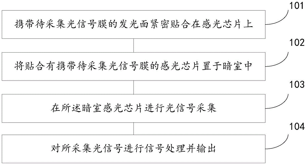
[0058] refer to figure 1, which shows a schematic flowchart of an embodiment of a method for collecting signals by a photosensitive chip according to the present invention, which may specifically include the following steps:

[0059] Step 101, the light-emitting surface of the film carrying the optical signal to be collected is closely attached to the photosensitive chip;

[0060] In practical applications, when using a photosensitive chip to collect western blot signals, the acquisition of the membrane carrying the light signal to be collected includes the following steps:

[0061] Run the electrophoresis of the protein to be tested first;

[0062] After running the electrophoresis gel for protein transfer;

[0063] Transfer the protein to be tested in the gel to polyvinylidene fluoride membrane or nitrocellulose membrane;

[0064] ...

Embodiment 2

[0104] A device for collecting signals by a photosensitive chip provided by an embodiment of the present invention is introduced in detail.

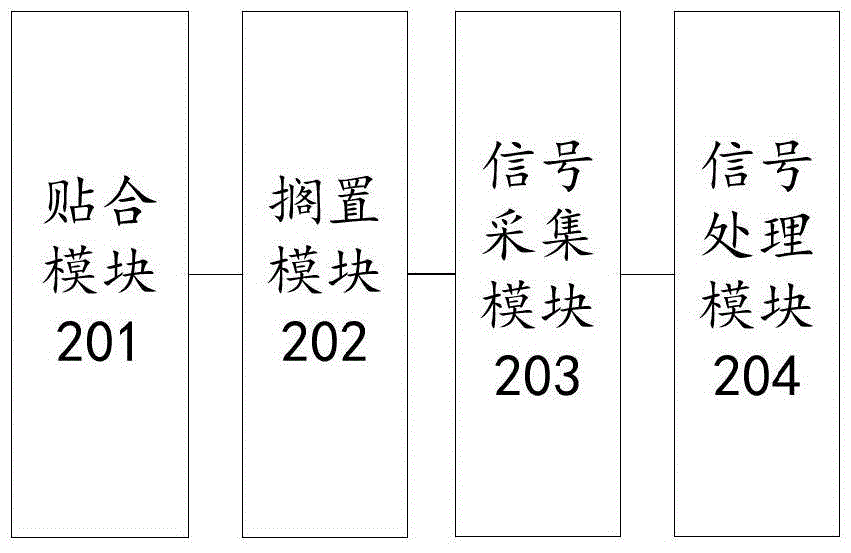
[0105] see figure 2 , which shows a schematic structural diagram of a device for collecting signals by a photosensitive chip of the present invention, specifically including:

[0106] A bonding module 201, configured to closely bond the light-emitting surface carrying the optical signal film to be collected on the photosensitive chip;

[0107] The shelving module 202 is used to place the photosensitive chip bonded with the film carrying the light signal to be collected in a dark room; the dark room is not affected by external light;

[0108] A signal collection module 203, configured to complete light signal collection on the photosensitive chip in the darkroom;

[0109] The signal processing module 204 is configured to perform signal processing on the collected optical signal and output it.

[0110] As for the device embodiment, sin...

Embodiment 3

[0112] A method for tracking cells with a photosensitive chip provided by an embodiment of the present invention is introduced in detail.

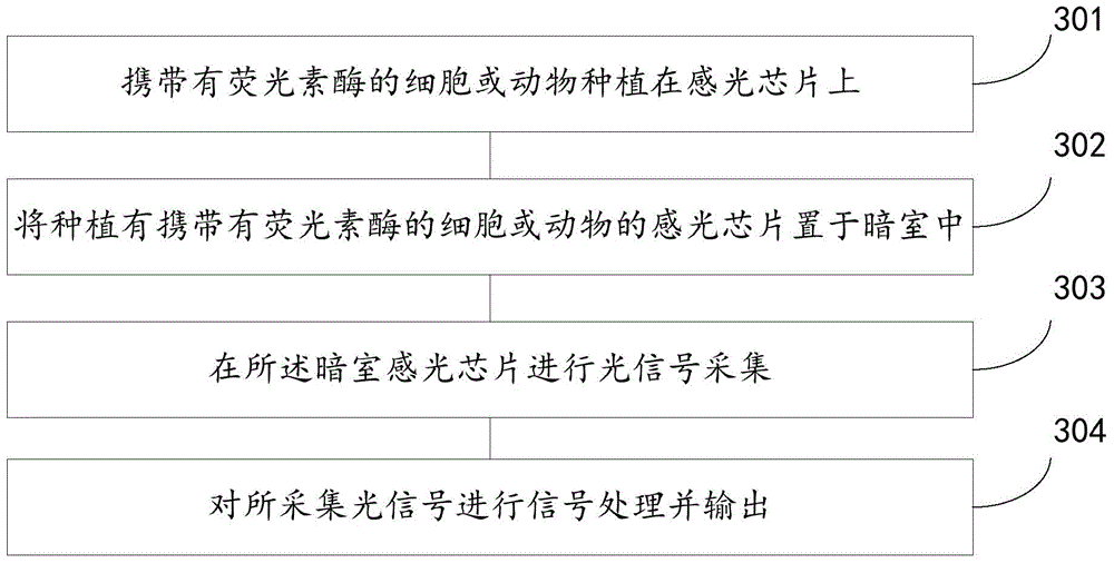
[0113] refer to image 3 , showing a method for tracking cells with a photosensitive chip of the present invention, which may specifically include:

[0114] Step 301, cells or animals carrying luciferase are planted on the photosensitive chip;

[0115] The photosensitive chip is usually covered with a transparent protective layer, or a glass layer or a resin layer or other materials, etc., and the thickness of the protective layer is usually less than 0.5mm.

[0116] In practice, considering the tracking effect and the secondary use of the photosensitive chip, a glass layer can be added to the photosensitive chip before the cells or animals carrying luciferase are planted on the photosensitive chip, and then the cells carrying luciferase Or animals are planted on the glass layer of the photosensitive chip, which will be more convenient i...


PUM


Abstract

The invention discloses methods and devices for acquiring signals and tracking cells by adopting light sensitive chips, and relates to the technical field of signal acquisition. The signal acquiring method adopting the light sensitive chip comprises the following steps: a light-emitting surface carrying a to-be-acquired light signal film is tightly attached to the light sensitive chip, the light sensitive chip attached with the to-be-acquired light signal film is placed in a darkroom, and the light sensitive chip acquires light signals in the darkroom, processes the acquired light signals and outputs the signals. The signal acquiring method and device adopting the light sensitive chip acquire the signals by the aid of contact with the light sensitive chip, the light signals are converted into digital signals, and quantitative analysis is finished very well.

Description

technical field [0001] The invention relates to the technical field of information collection, in particular to a method and device for collecting signals by a photosensitive chip and a method and device for tracking cells. Background technique [0002] Western blotting is a hybridization technique that combines high-resolution gel electrophoresis and immunochemical analysis techniques. Western blotting has the advantages of large analysis capacity, high sensitivity, and strong specificity. It is the most commonly used method for detecting protein characteristics, expression, and distribution, such as qualitative and quantitative detection of tissue antigens, mass determination of polypeptide molecules, and detection of viruses. Antibody or antigen detection, etc. [0003] Existing devices and methods for collecting Western blotting signals: [0004] Method 1: Put the photosensitive film and the NC film close together, after exposing for a certain period of time, develop a...

Claims


Application Information

Patent Timeline
Patent Type & Authority Applications(China)
IPC IPC(8): G01N33/68G01N33/544C12Q1/66
CPCC12Q1/66G01N33/544G01N33/68G01N21/76C09K11/61G01N21/763G01N33/561G01N2021/1765G01N2001/4038G01N33/52G01N33/535G01N33/543G01N33/6842
Inventor 张英豪詹克团宛佳张志豪
Owner SANGHAI E BLOT PHOTOELECTRIC TECHNOLOGY CO LTD
Learn More