
Method for manufacturing liquid crystal display device

A technology of liquid crystal display device and manufacturing method, which is applied in nonlinear optics, instruments, optics, etc., can solve problems such as high cost, harm to human body, and not obvious improvement effect, and achieve the goal of avoiding mura, avoiding abnormality, and simple process Effect

Active Publication Date: 2018-05-29
KUSN INFOVISION OPTOELECTRONICS
View PDF4 Cites 0 Cited by
  • Summary
  • Abstract
  • Description
  • Claims
  • Application Information

AI Technical Summary

Problems solved by technology

However, for Method 1, the cost of replacing the exposure machine for black ceramics is very high, with an average cost of about 3.1 million RMB per unit. However, the improvement effect of Method 2 is not obvious, and the cost is too high. Method 3 Non-reflective electrostatic fluid is harmful to the human body and is easy to corrode the exposure machine

Method used

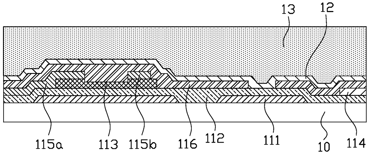
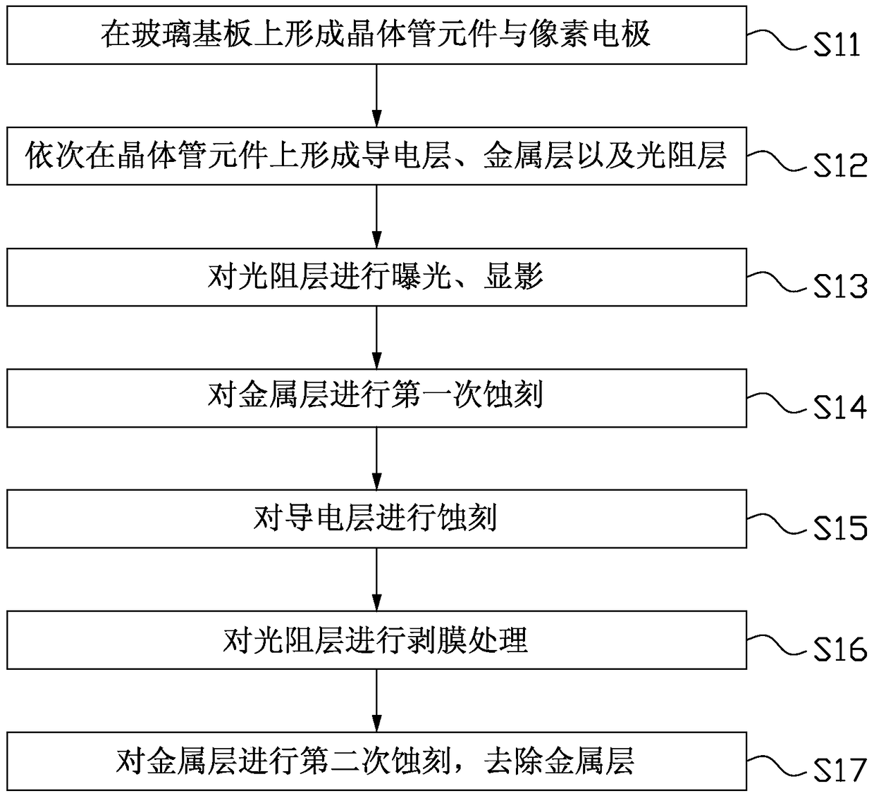
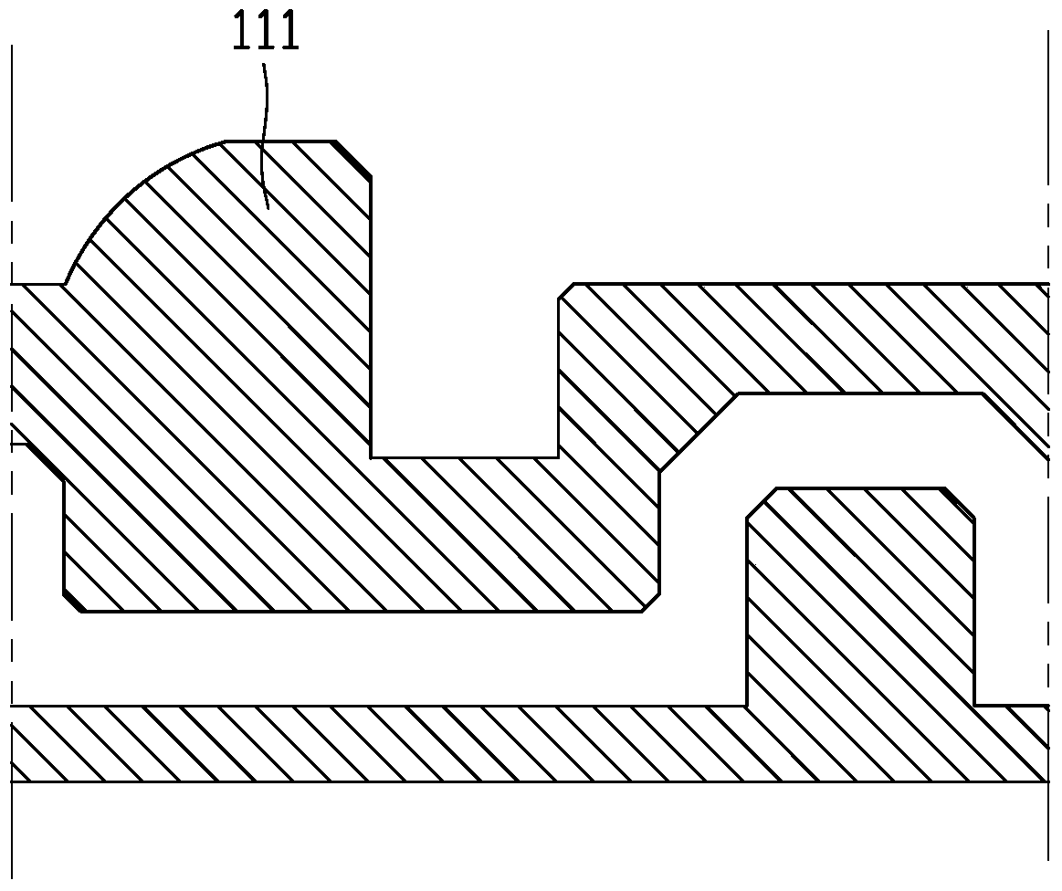

Image

  • Method for manufacturing liquid crystal display device
  • Method for manufacturing liquid crystal display device
  • Method for manufacturing liquid crystal display device

Examples


Embodiment Construction

[0025] In order to further illustrate the technical means and effects that the present invention adopts to achieve the intended purpose of the invention, below in conjunction with the accompanying drawings and preferred embodiments, the specific implementation methods, methods, steps, The structure, characteristics and functions are described in detail below.

[0026] The foregoing and other technical contents, features and effects of the present invention will be clearly presented in the following detailed description of preferred embodiments with reference to the drawings. Through the description of specific implementation methods, the technical means and effects of the present invention to achieve the intended purpose can be understood more deeply and specifically, but the attached drawings are only for reference and description, and are not used to explain the present invention limit.

[0027] Please also refer to figure 2 , Figure 3a to Figure 3e and Figures 4a to ...


PUM

PropertyMeasurementUnit
thicknessaaaaaaaaaa
thicknessaaaaaaaaaa
thicknessaaaaaaaaaa

Abstract

The invention provides a method for manufacturing a liquid crystal display apparatus. The method comprises steps of forming transistor elements and pixel electrodes on a glass substrate, sequentially forming a conductive layer, a metal layer and a light resistance layer on the transistor elements, exposing and developing the light resistance layer, firstly etching the metal layer, etching the conductive layer, peeling the light resistance layer, and secondly etching the metal layer to remove the metal layer. In the method for manufacturing the liquid crystal display apparatus, a metal layer is added on the conductive layer, light cannot emit to an exposure machine bench through a transparent conductive layer during exposure, mura, caused by reflection of the exposure machine bench, on an array substrate can be avoided, and the process is simple and the cost is low.

Description

technical field [0001] The invention relates to the technical field of liquid crystal display, in particular to a method for manufacturing a liquid crystal display device. Background technique [0002] A liquid crystal display (Liquid Crystal Display, LCD) has many advantages such as thinness, energy saving, and no radiation, so it has gradually replaced the traditional cathode ray tube (CRT) display. Currently, liquid crystal displays are widely used in high-definition digital televisions, desktop computers, personal digital assistants (PDAs), notebook computers, mobile phones, digital cameras and other electronic devices. [0003] Common liquid crystal displays can be divided into narrow viewing angle twisted nematic (Twisted Nematic, TN) LCD, super twisted nematic (Super Twisted Nematic, STN) LCD, double layer super twisted nematic (Double layer Super Twisted Nematic, DSTN) LCD and wide viewing angle fringe field switching technology (Fringe Field Switching, FFS) LCD, in...

Claims


Application Information

Patent Timeline
Patent Type & Authority Patents(China)
IPC IPC(8): G02F1/13
CPCG02F1/1303
Inventor 张庆明张波
Owner KUSN INFOVISION OPTOELECTRONICS
Learn More