
Waste elimination mechanism of automatic PCB sorting machine

An automatic sorting and PCB board technology, applied in the field of mechanical equipment, can solve the problems of unable to collect the bottom image of the PCB board, out of synchronization, etc., achieve the effect of high recognition rate and reduce equipment cost

Active Publication Date: 2015-09-02
NORTHEASTERN UNIV
View PDF8 Cites 10 Cited by
  • Summary
  • Abstract
  • Description
  • Claims
  • Application Information

AI Technical Summary

Problems solved by technology

The use of the feeder can not only solve the problem of out-of-synchronization in the existing technology, but also reduce the manufacturing cost of the equipment, and it can also solve the problem that the current technology cannot collect the bottom image of the PCB board

Method used


Image

  • Waste elimination mechanism of automatic PCB sorting machine
  • Waste elimination mechanism of automatic PCB sorting machine
  • Waste elimination mechanism of automatic PCB sorting machine

Examples


Embodiment Construction

[0020] The present invention will be further described below in conjunction with the accompanying drawings and embodiments.

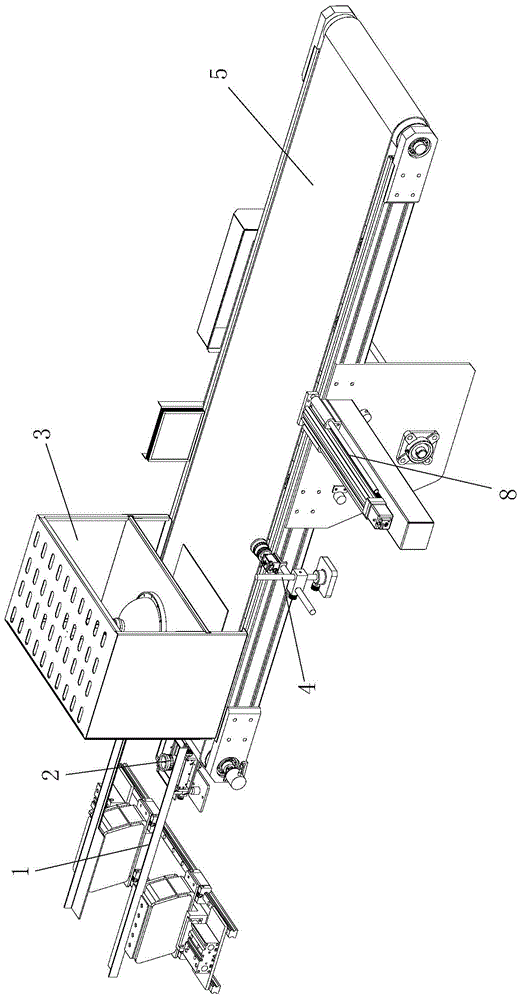
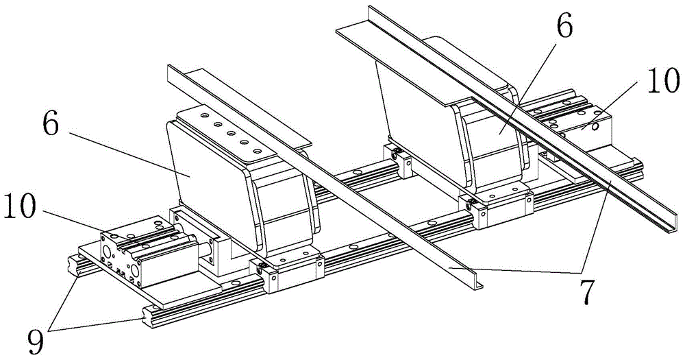
[0021] Embodiments of the present invention: a waste removal mechanism for an automatic PCB sorter, such as figure 1 As shown, it includes a linear transmission device 1, a bottom image acquisition device 2, a top image acquisition device 3, a side image acquisition device 4, and a conveyor belt 5. The linear transmission device 1 includes a feeder 6 and an "L"-shaped track 7, and 2 feeders 6 are provided with an "L"-shaped track 7 at the top, and the "L"-shaped track 7 is connected to the conveyor belt 5, and the bottom image acquisition device 2 is set at the middle position directly below the two "L"-shaped tracks 7, and the top image The acquisition device 3 is located at the junction of the conveyor belt 5 and the "L" shaped track 7, and is located above the conveyor belt 5; the side image acquisition device 4 is located on one side of the conveyor...


PUM


Abstract

The invention discloses a waste elimination mechanism of an automatic PCB sorting machine. The waste elimination mechanism comprises a linear conveying device, a bottom image collecting device, a top image collecting device, a side image collection device and a conveyor belt, wherein the linear conveying device comprises two feeders and L-shaped rails, each L-shaped rail is arranged at the top of each feeder and is connected with the conveyor belt; the bottom image collecting device is arranged in the middle right below the two L-shaped rails; the top image collecting device is arranged at the connecting parts among the conveyor belt and the L-shaped rails and is arranged above the conveyor belt; the side image collecting device is arranged at one side of the conveyor belt; a first push-pull cylinder is arranged on the side wall of the conveyor belt. The waste elimination mechanism is suitable for screening PCBs of various specifications, front face, back face and side face images of the PCBs can be accurately collected, the identification rate of defective products is increased and defective PCB can be automatically eliminated.

Description

technical field [0001] The invention relates to a rejecting device, in particular to a waste rejecting mechanism used in a PCB board automatic sorter, and belongs to the field of mechanical equipment. Background technique [0002] PCB boards are a necessity in the electronics industry. The traditional detection of PCB boards is generally manual detection. Manual detection is based on human observation and classification. The detection efficiency is extremely low and requires a lot of labor. cannot meet the needs of the times. It has become a big trend that machine inspection replaces manual inspection. The theoretical basis of machine inspection is image processing, at least taking pictures of both sides of the PCB board. [0003] It is difficult to realize the image acquisition of the PCB board with one conveyor belt, so the traditional conveyor belt will use two conveyor belts to transport the PCB board in a bridge type, which can meet the requirements of the lower surfa...

Claims


Application Information

Patent Timeline
Patent Type & Authority Applications(China)
IPC IPC(8): B07C5/34B07C5/02
Inventor 马振鹤姚学练张成龙杨鹏李琛杜文帅
Owner NORTHEASTERN UNIV
Learn More