Pixel drive circuit and method, array substrate and display device

A technology of a pixel driving circuit and a driving unit, which is applied in the fields of array substrates, display devices, driving methods, and pixel driving circuits, can solve the problems of reducing the lifespan of driving TFTs, shortening the lifespan of OLED display panels, etc., so as to ensure brightness uniformity and avoid luminescence. The effect of the effect of brightness

Active Publication Date: 2015-03-25
HEFEI XINSHENG OPTOELECTRONICS TECH CO LTD +1
View PDF10 Cites 12 Cited by
  • Summary
  • Abstract
  • Description
  • Claims
  • Application Information

AI Technical Summary

Problems solved by technology

In addition, during the working process of the OLED, the driving TFT is always in the conduction state, and long-time work will reduce the life of the driving TFT, and correspondingly reduce the life of the OLED display panel.

Method used


Image

  • Pixel drive circuit and method, array substrate and display device
  • Pixel drive circuit and method, array substrate and display device
  • Pixel drive circuit and method, array substrate and display device

Examples


Embodiment Construction

[0033] The technical solutions in the embodiments of the present disclosure will be clearly and completely described below in conjunction with the accompanying drawings. Apparently, the described embodiments are part of the embodiments of the present disclosure, but not all of the embodiments.

[0034] In the present disclosure, when it is described that a specific device is located between a first device and a second device, there may or may not be an intervening device between the specific device and the first device or the second device; when describing When a specific device is connected to other devices, the specific device may be directly connected to the other device without an intermediate device, or may not be directly connected to the other device but has an intermediate device.

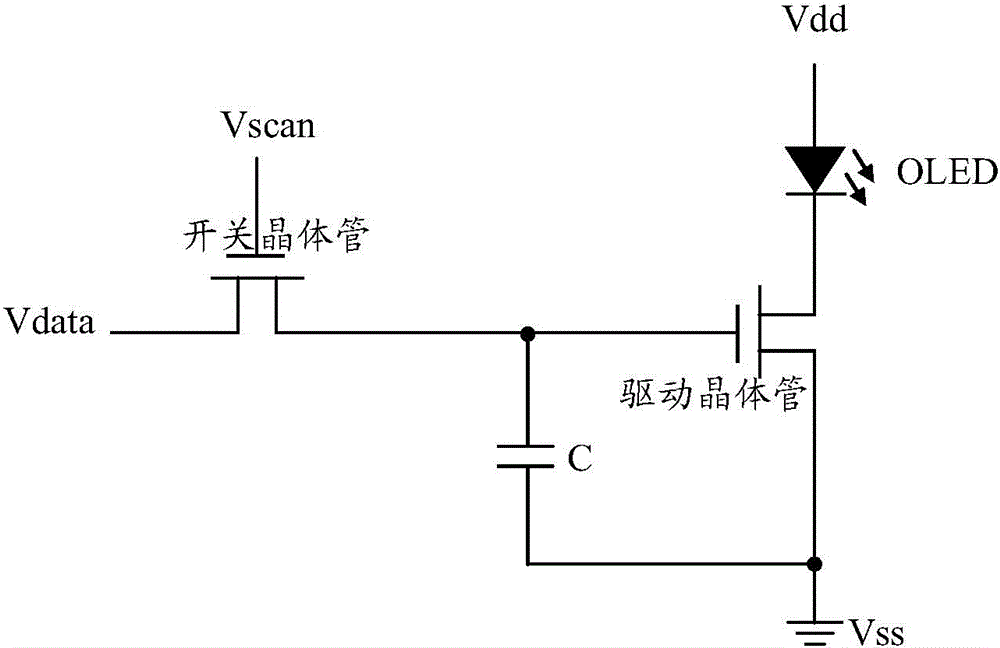
[0035] figure 1 is a circuit diagram schematically illustrating a conventional 2T1C drive circuit for OLEDs. Such as figure 1 As shown, the 2T1C driving circuit includes a switching trans...


PUM


Abstract

The invention provides a pixel drive circuit and method, an array substrate and a display device. A first drive assembly in the pixel drive circuit comprises a first switching unit, a first charging unit, a first drive unit and a first drive compensation unit. The first switching unit is switched on or off according to first scanning signals so as to control transmission of data signals. The first end of the first charging unit is connected with the second end of the first switching unit. The control end of the first drive unit is connected to the second end of the first charging unit, the first end of the first drive unit is connected to a first power source through a light-emitting device, and the second end of the first drive unit is connected to a second power source. The first drive compensation unit is used for generating preset voltages at the control end of the first drive unit when the first switching unit is switched on according to the first scanning signals, and currents flowing through the light-emitting device are irrelevant to threshold voltages of the first drive unit through the preset voltages. By the adoption of the technical scheme, the influences of the threshold voltages for driving transistors on light-emitting brightness are avoided, and brightness uniformity of the light-emitting device is guaranteed.

Description

technical field [0001] The present disclosure relates to the field of display technology, and more specifically, to a pixel driving circuit, a driving method, an array substrate and a display device. Background technique [0002] With the advancement of display technology, light emitting diode (light emitting diode, LED) display panels are gradually entering the market, which typically include active matrix organic light emitting diode (Active Matrix Organic Light Emitting Diode, AMOLED). Compared with the traditional liquid crystal display (Liquid Crystal Display, LCD) technology, AMOLED display has faster response speed, higher contrast ratio and wider viewing angle, and does not require a backlight unit, so AMOLED display is considered to be the next generation display technology . In AMOLED, the light-emitting device is an organic light-emitting diode (Organic Light-Emitting Diode, OLED). Driven by the AMOLED driving circuit, when a current flows through the light emit...

Claims


Application Information

Patent Timeline
Patent Type & Authority Applications(China)
IPC IPC(8): G09G3/32G09G3/3225
CPCG09G3/3225G09G2300/0814G09G2300/0819G09G2320/045
Inventor 胡祖权
Owner HEFEI XINSHENG OPTOELECTRONICS TECH CO LTD
Why Eureka
Try Eureka