Fingerprint identification chip packaging method and packaging structure

A chip packaging structure, fingerprint recognition technology, applied in character and pattern recognition, acquisition/organization of fingerprints/palmprints, electrical components, etc., can solve the problems of fingerprint recognition device manufacturing and application limitations, high sensitivity requirements of fingerprint recognition chips, etc. Achieve the effect of reducing sensitivity, wide application and process simplification

Active Publication Date: 2018-04-20
CHINA WAFER LEVEL CSP
View PDF5 Cites 0 Cited by
  • Summary
  • Abstract
  • Description
  • Claims
  • Application Information

AI Technical Summary

Problems solved by technology

[0005] However, in the existing fingerprint identification devices, the sensitivity of the fingerprint identification chip is required to be high, which limits the manufacture and application of fingerprint identification devices.

Method used


Image

  • Fingerprint identification chip packaging method and packaging structure
  • Fingerprint identification chip packaging method and packaging structure
  • Fingerprint identification chip packaging method and packaging structure

Examples


Embodiment Construction

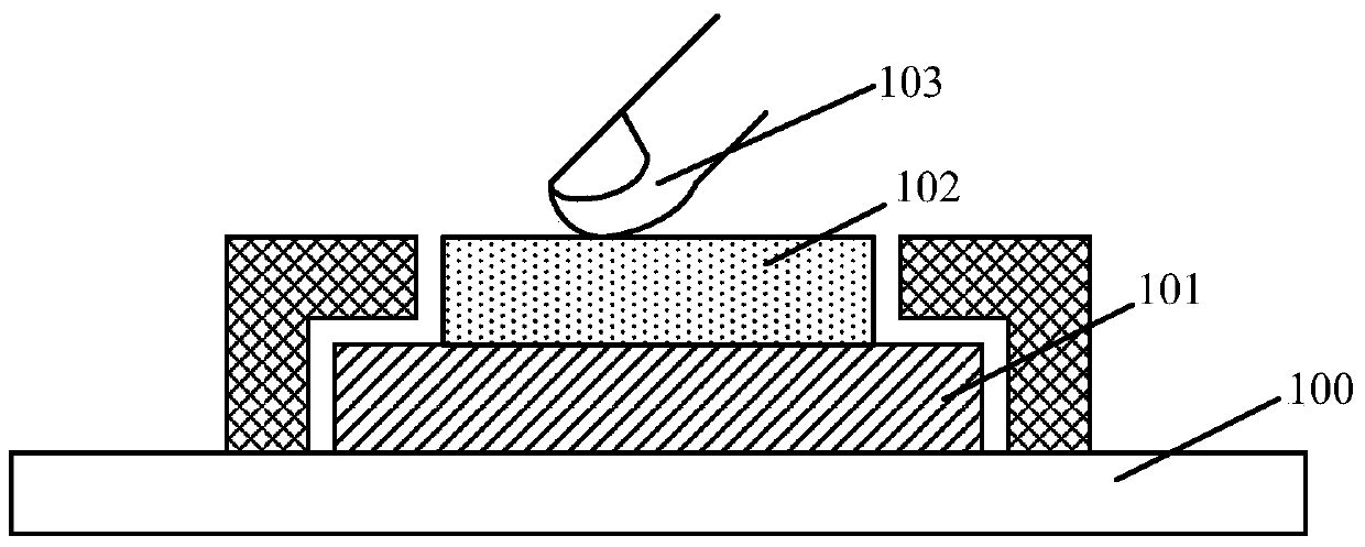
[0065] As mentioned in the background, in the existing fingerprint identification devices, the sensitivity of the fingerprint identification chip is required to be high, so that the manufacture and application of the fingerprint identification devices are limited.

[0066] After research, please continue to refer to figure 1 , the surface of the fingerprint identification chip 101 is covered with a glass substrate 102, the glass substrate 102 is used to protect the fingerprint identification chip 101, and the user's finger 103 is directly in contact with the glass substrate 102, therefore, in order to ensure that the glass substrate 102 has For sufficient protection capability, the thickness of the glass substrate 102 is relatively thick. However, since the glass substrate 102 is relatively thick, the fingerprint recognition chip 101 is required to have high sensitivity to ensure that the user's fingerprint can be accurately extracted. However, it is difficult to manufacture ...


PUM


Abstract

A fingerprint identification chip packaging method and packaging structure, wherein the packaging method includes: providing a substrate; coupling an induction chip on the surface of the substrate, the induction chip has a first surface and a second surface opposite to the first surface, the The first surface of the sensing chip includes a sensing area, the second surface of the sensing chip is located on the surface of the substrate; a plastic sealing layer is formed on the surface of the substrate, the plastic sealing layer surrounds the sensing chip, and the surface of the plastic sealing layer is in contact with the The first surface of the sensing chip is flush; a covering layer is formed on the plastic encapsulation layer and the first surface of the sensing chip, and the thickness of the covering layer is less than 100 microns. The packaging structure of the fingerprint identification chip formed by the packaging method is simplified, which can reduce the requirement on the sensitivity of the sensing chip, and make the packaging method and the packaging structure more widely used.

Description

technical field [0001] The invention relates to the technical field of semiconductor manufacturing, in particular to a fingerprint identification chip packaging method and packaging structure. Background technique [0002] With the progress of modern society, the importance of personal identification and personal information security has gradually attracted people's attention. Due to the uniqueness and invariance of human fingerprints, fingerprint identification technology has the characteristics of good security, high reliability, and simple and convenient use, making fingerprint identification technology widely used in various fields to protect personal information security. With the continuous development of science and technology, the information security of various electronic products has always been one of the key points of technological development. Especially for mobile terminals, such as mobile phones, notebook computers, tablet computers, digital cameras, etc., th...

Claims


Application Information

Patent Timeline
Patent Type & Authority Patents(China)
IPC IPC(8): H01L21/56H01L21/60H01L23/31H01L23/498
CPCH01L21/56H01L23/293H01L23/3121H01L23/49811H01L2224/73265H01L2224/48091H01L2924/00014H01L23/498H01L2924/181H01L2924/10155H01L23/32H01L23/60H01L24/32H01L24/48H01L24/73H01L2224/04042H01L2224/32225H01L2224/32245H01L2224/48227H01L2224/48247H01L24/45H01L2224/24227H01L2224/24246H01L24/24H01L2224/45147H01L2224/45139H01L2224/45144H01L2224/45184H01L2224/45124G06V40/1306H01L2924/00012H01L23/31H01L23/04H01L23/08H01L23/3128H01L23/585H01L24/19H01L2924/00
Inventor 王之奇喻琼王蔚
Owner CHINA WAFER LEVEL CSP
Why Eureka
Try Eureka