Pixel structure and display panel with same

A pixel structure and display panel technology, applied in the direction of instruments, semiconductor devices, optics, etc., can solve the problem of increasing the overlapping area of ​​scanning lines and data lines and the first metal layer, shorting of scanning lines and data lines, and rising product costs, etc. problem, to achieve low color shift, reduce the probability of short circuit, and save cost

Inactive Publication Date: 2014-09-24
TCL CHINA STAR OPTOELECTRONICS TECH CO LTD
View PDF5 Cites 13 Cited by
  • Summary
  • Abstract
  • Description
  • Claims
  • Application Information

AI Technical Summary

Problems solved by technology

[0004] In the process of implementing the present invention, the inventors of the present invention found at least the following technical defects in the prior art: In the above-mentioned design, the shared TFT is generally driven by the scanning line in the sub-pixel area. , the scanning line of the sub-pixel area of ​​the Nth pixel area will be connected with the scanning line of the main pixel area of ​​the N+1, N+2, N+3 or N+4th pixel area, thus not only It greatly affects the aperture ratio, and also increases the overlapping area of ​​the scanning line, the data line and the first metal layer, which increases the probability of short-circuiting of the scanning line and the data line, resulting in a substantial increase in product cost

Method used


Image

  • Pixel structure and display panel with same
  • Pixel structure and display panel with same
  • Pixel structure and display panel with same

Examples


Embodiment Construction

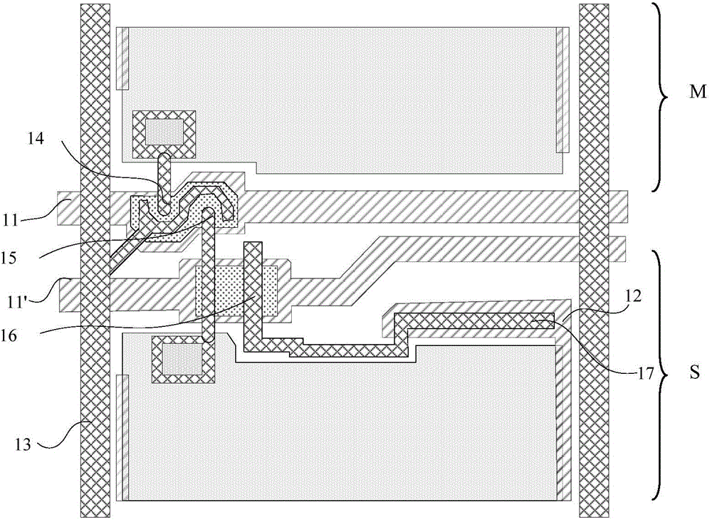
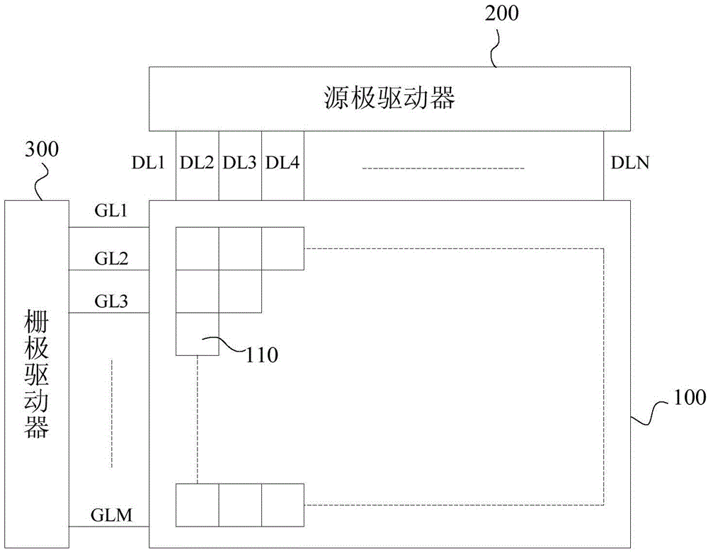
[0024] The implementation of the present invention will be described in detail below in conjunction with the accompanying drawings and examples, so as to fully understand and implement the process of how to apply technical means to solve technical problems and achieve technical effects in the present invention. It should be noted that, as long as there is no conflict, each embodiment and each feature in each embodiment of the present invention can be combined with each other, and the formed technical solutions are all within the protection scope of the present invention.

[0025] The following descriptions of the various embodiments refer to the accompanying drawings to illustrate specific embodiments in which the present invention can be practiced. The directional terms mentioned in the present invention, such as "upper", "lower", "left", "right", etc., are only referring to the directions of the attached drawings. Therefore, the directional terms used are used to illustrate ...


PUM


Abstract

The invention discloses a pixel structure and a display panel with the same. The pixel structure comprises multiple sub-pixels, wherein each sub pixel comprises a first display area and a second display area, each first display area is used for receiving a scanning signal of a scanning line and further receiving a data signal of a data line and has a first potential, and each second display area is used for receiving the scanning signal of the scanning line and further receiving the data signal of the data line; each second display area is used for receiving a voltage signal of a public line and pulling the voltage obtained by the data signal of the data line down to a second potential; a voltage difference exists between the second potential and the first potential. The pixel structure can be used for reducing the short circuit possibility of the scanning line and the data line without sacrificing the aperture rate under the condition of wide view angle.

Description

technical field [0001] The present invention relates to the field of liquid crystal display technology, in particular to a pixel structure and a display panel with the pixel structure. Background technique [0002] With the development of the information society, people's demand for display equipment has been increased, thus also promoting the rapid development of the liquid crystal display panel industry. The display specifications of liquid crystal display panels are constantly developing toward large sizes. In order to overcome the viewing angle problem under large-size display specifications, the wide viewing angle technology of liquid crystal display panels must also be improved and broken through. [0003] At present, there is a wide viewing angle design in this field, which is to divide a pixel into a main pixel area and a sub-pixel area, and pull down the voltage of the sub-pixel area by sharing a thin film transistor (TFT for short) and a pull-down capacitor, thereb...

Claims


Application Information

Patent Timeline
Patent Type & Authority Applications(China)
IPC IPC(8): G02F1/1362G02F1/1343
CPCG02F1/13624G02F1/134345G02F1/136213G02F1/136286G02F1/1368G02F2201/123H01L29/78696
Inventor 柴立
Owner TCL CHINA STAR OPTOELECTRONICS TECH CO LTD
Why Eureka
Try Eureka