Polycrystalline silicon film morphology forming method

A polysilicon and film technology, applied in electrical components, semiconductor/solid-state device manufacturing, semiconductor devices, etc., can solve the problem of inconsistency in the longitudinal width of polycrystalline strips, achieve uniform longitudinal width, reduce or eliminate narrow edges. Effect

Active Publication Date: 2014-07-23
SHANGHAI INTEGRATED CIRCUIT RES & DEV CENT
View PDF8 Cites 5 Cited by
  • Summary
  • Abstract
  • Description
  • Claims
  • Application Information

AI Technical Summary

Problems solved by technology

[0006] The technical problem to be solved by the present invention is to provide a method for forming the morphology of polysilicon film layer to solve the problem of uniformity of polysilicon gate morphology, such as the narrow side of the polysilicon strip formed by etching, the polysilicon strip in the vertical direction Inconsistent upper width and other issues

Method used


Image

  • Polycrystalline silicon film morphology forming method
  • Polycrystalline silicon film morphology forming method
  • Polycrystalline silicon film morphology forming method

Examples


Embodiment 1

[0033] figure 1 It is a schematic flow chart of a method for forming a polysilicon film layer morphology in an embodiment of the present invention; as figure 1 As shown, it can specifically include:

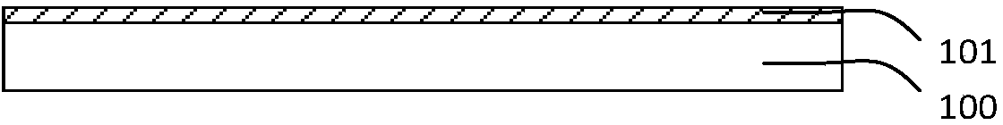
[0034] S101, forming a gate oxide layer on the substrate;

[0035] In this embodiment, the gate oxide layer may be formed by thermally oxidizing the substrate. The thickness of the gate oxide layer is 50-200A, preferably 100A. For details, see figure 2 , figure 2 It is a schematic diagram of the structure of the semi-finished product after step S101 according to Embodiment 1 of the present invention. A gate oxide layer 101 has been formed on the substrate 100 .

[0036] It should be noted that the formation of the gate oxide layer is not limited to the method of thermally oxidizing the substrate, and other methods may also be used according to process requirements.

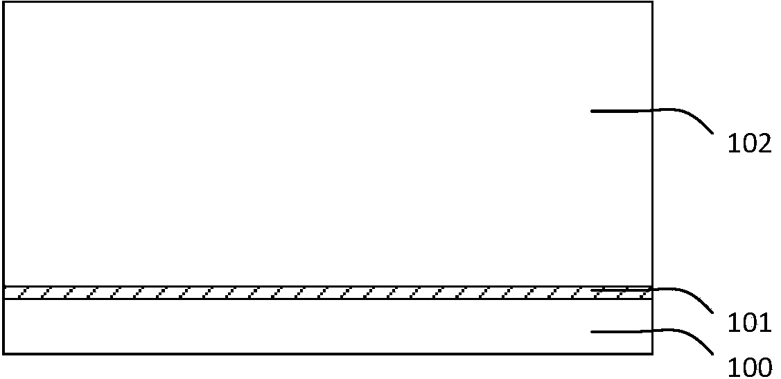
[0037] S102, forming a polysilicon film layer on the gate oxide layer;

[0038] In this embodiment, consi...


PUM


Abstract

The invention discloses a polycrystalline silicon film morphology forming method and belongs to the technical field of semiconductors. The polycrystalline silicon film morphology forming method comprises the steps of forming a grid electrode oxidation layer on a substrate and forming a polycrystalline silicon film layer on the grid electrode oxidation layer; performing doping treatment on the polycrystalline silicon film layer on the grid electrode oxidation layer; performing etching treatment on the polycrystalline silicon film layer subjected to the doping treatment according to the doping concentration distribution of the polycrystalline silicon film layer subjected to the doping treatment so as to form even polycrystalline silicon film morphology. In the polycrystalline silicon film morphology forming method, the transverse etching degree is influenced by adjusting the etching gas flow ratio or step-by-step etching according to the doping concentration distribution of the polycrystalline silicon film layer subjected to the doping treatment, accordingly the polycrystalline strip narrow edge situation is relieved or eliminated, even polycrystalline strips identical in longitudinal width are obtained, and follow-up process implementation is facilitated.

Description

technical field [0001] The invention belongs to the technical field of semiconductors, and in particular relates to a method for forming the morphology of a polysilicon film layer. Background technique [0002] The manufacturing process of the existing field effect transistor is roughly as follows: after forming the gate insulating layer on the substrate, then forming a polysilicon film layer as the gate film layer; then doping the polysilicon film layer to improve its conductivity, and then doping the polysilicon film layer The film layer is patterned to form a gate structure, and finally the substrate materials on both sides of the gate are doped to form a source region and a drain region respectively, thereby finally completing the manufacture of a field effect transistor. [0003] In the manufacturing process of the above-mentioned field effect transistor, since the polycrystalline gate structure will directly affect the main electrical properties of the MOS transistor, ...

Claims


Application Information

Patent Timeline
Patent Type & Authority Applications(China)
IPC IPC(8): H01L21/28
CPCH01L21/32137H01L21/32155H01L29/42376
Inventor 王伟军奚鹏程杨冰
Owner SHANGHAI INTEGRATED CIRCUIT RES & DEV CENT
Why Eureka
Try Eureka