Optical imaging lens and electronic device using the optical imaging lens

An optical imaging lens and imaging technology, applied in the field of optical lenses, to achieve the effect of shortening the system length, meeting consumer demand, and good optical performance

Active Publication Date: 2016-05-11
GENIUS ELECTRONICS OPTICAL XIAMEN
View PDF6 Cites 2 Cited by
  • Summary
  • Abstract
  • Description
  • Claims
  • Application Information

AI Technical Summary

Problems solved by technology

[0003] U.S. Patent No. 7,580,205 discloses a wide-angle optical lens composed of six lenses. The length of the lens is as long as 2 centimeters. Such an oversized lens cannot be used for electronic devices that are only 1 to 2 centimeters thin in pursuit of thinness and shortness. device

Method used


Image

  • Optical imaging lens and electronic device using the optical imaging lens
  • Optical imaging lens and electronic device using the optical imaging lens
  • Optical imaging lens and electronic device using the optical imaging lens

Examples


Embodiment Construction

[0110] The present invention will now be further described with reference to the drawings and specific embodiments.

[0111] Before the present invention is described in detail, it should be noted that in the following description, similar components are represented by the same numbers.

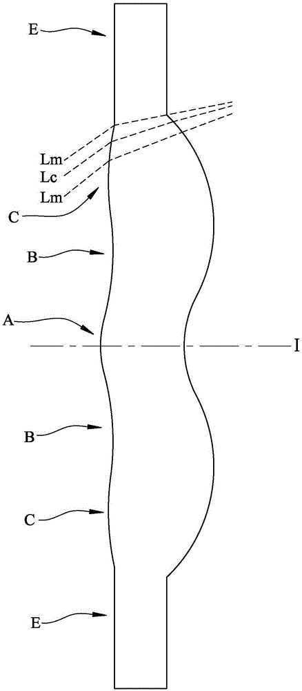
[0112] In this specification, "a lens has positive refractive power (or negative refractive power)" means that the lens has positive refractive power (or negative refractive power) in the area near the optical axis. “The object side (or image side) of a lens has a convex surface (or concave surface) located in a certain area” means that this area is more oriented parallel to the optical axis than the area immediately outside the area in the radial direction. "Outwardly convex" (or "inwardly concave"), in terms of figure 1 For example, where I is the optical axis and this lens is radially symmetrical with the optical axis I as the symmetry axis, the object side of the lens has a convex surface in a...


PUM


Abstract

The invention relates to an optical imaging lens and an electronic device applying the optical imaging lens. The optical imaging lens sequentially comprises six lenses from an objective side to an image side, wherein an objective side face of the first lens is provided with a convex face portion located in an area nearby an optical axis, and an image side face is provided with a concave face portion located in an area nearby the optical axis; an image side face of the second lens is provided with a convex face portion located in an area nearby the optical axis; an objective side face of the third lens is provided with a convex face portion located in an area nearby the optical axis; an objective side face of the fifth lens is provided with a convex face portion located in an area nearby a circumference, and an image side face is provided with a convex face portion located in an area nearby the optical axis; and an image side face of the sixth lens is provided with a concave face portion located in an area nearby the optical axis. The electronic device comprises a casing and an image module, wherein the image module comprises the optical imaging lens, a lens cone, a module rear base unit and an image sensor. The electronic device applying the optical imaging lens has the advantages of imaging qualify improvement and miniaturization by being matched with the lens.

Description

Technical field [0001] The invention relates to an optical lens, in particular to an optical imaging lens and an electronic device using the optical imaging lens. Background technique [0002] In recent years, the popularization of portable electronic products such as mobile phones and digital cameras has led to the rapid development of image module related technologies. The image module mainly includes components such as optical imaging lenses, moduleholder units, and sensors. The trend toward thinner and lighter cameras has also increased the demand for miniaturization of image modules. With the technological advancement of ChargeCoupled Device (CCD) or Complementary Metal-Oxide Semiconductor (Complementary Metal-Oxide Semiconductor, CMOS) In order to reduce the size of the optical imaging lens, the length of the optical imaging lens mounted in the image module needs to be shortened accordingly. However, in order to avoid the deterioration of the photographic effect and quality...

Claims


Application Information

Patent Timeline
Patent Type & Authority Patents(China)
IPC IPC(8): G02B13/18G02B13/00
Inventor 廖陈成
Owner GENIUS ELECTRONICS OPTICAL XIAMEN
Why Eureka
Try Eureka