Bonding tool detection method

A detection method and technology of bonding tools, which are applied in the direction of manufacturing tools, measuring devices, metal processing equipment, etc., can solve problems such as unqualified detection of bonding tools, failure to judge MEMS devices, etc., and achieve the effect of avoiding product waste

Active Publication Date: 2014-04-16
SEMICON MFG INT (SHANGHAI) CORP
View PDF7 Cites 7 Cited by
  • Summary
  • Abstract
  • Description
  • Claims
  • Application Information

AI Technical Summary

Problems solved by technology

[0005] The problem solved by the present invention is that the existing technology cannot detect whether the bonding tool in the metal bonding technology is qualified before bonding, and it is impossible to judge whether the subsequent metal bonding process using the bonding tool can obtain a higher pass rate. High MEMS Devices

Method used


Image

  • Bonding tool detection method
  • Bonding tool detection method
  • Bonding tool detection method

Examples


Embodiment Construction

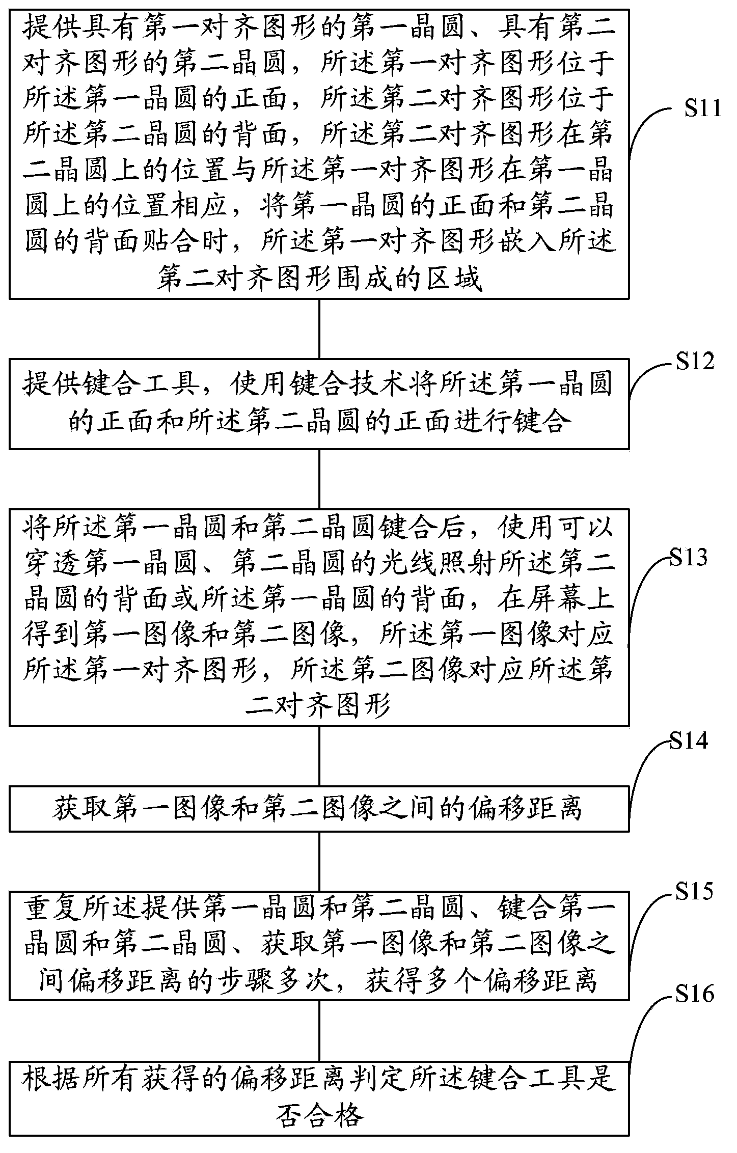
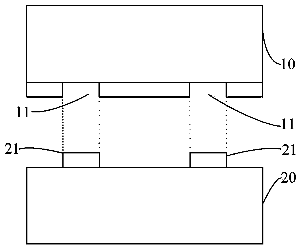
[0040]The inventors conducted research on defective MEMS device products obtained by using bonding tools in metal bonding technology, and found that: during the metal bonding process, when using bonding tools to press metal and wafer or metal and metal , it will cause the bonding contact points between metal and metal, or metal and wafer are not completely aligned, that is, the metal is offset relative to the wafer or one of the metals relative to the other metal during the bonding process, so that The resulting product will not function properly due to poor contact at the bonding contacts. Furthermore, the bonded contacts are prone to breakage, rendering the product inoperable. The inventor has noticed that the reason for the bonding offset is mainly that there is a problem with the bonding tool itself, such as in the bonding tool, the contact between metal and metal or metal and wafer is closer and firm. Or the size and direction of the pressure exerted by the metal are une...


PUM


Abstract

A bonding tool detection method includes the steps of firstly, providing an area, wherein the area is provided with a first wafer with a first alignment pattern and a second wafer with a second alignment pattern, and the area is formed in a surrounding mode by embedding the first alignment pattern into the second alignment pattern when the front face of the first wafer is attached to the back face of the second wafer; secondly, providing a bonding tool so that the front face of the first wafer and the front face of the second wafer can be bonded; thirdly, conducting illumination through light rays, and obtaining a first image and a second image on a screen; fourthly, obtaining the offset distance between the first image and the second image; fifthly, repeatedly executing the step of providing the first wafer and the second wafer, the step of bonding the first water and the second wafer and the step of obtaining the offset distance between the first image and the second image, and obtaining a plurality of offset distances; sixthly, judging whether the bonding tool is qualified or not according to all the obtained offset distances. By means of the bonding tool detection method, whether the bonding tool is qualified or not can be accurately judged before the bonding tool is applied to the actual bonding technology, and unnecessary product waste is avoided.

Description

technical field [0001] The invention relates to the technical field of microelectronics, in particular to the field of MEMS bonding technology. Background technique [0002] Microelectromechanical systems (MEMS for short) is a cutting-edge multidisciplinary research field developed on the basis of microelectronics technology. It is a technology that uses semiconductor technology to manufacture microelectromechanical devices. In the MEMS processing technology, the bonding technology is the key process, and the metal bonding technology in the bonding technology is a commonly used bonding technology. Metal bonding refers to the face-to-face bonding of two MEMS devices through pure metals or alloys, relying on metal bonds, diffusion between the metal and the surface of the MEMS device, and metal melting. [0003] However, the performance of the MEMS device obtained by performing the metal bonding technology using the prior art bonding tools may be poor. Moreover, in the prior ...

Claims


Application Information

Patent Timeline
Patent Type & Authority Applications(China)
IPC IPC(8): G01B11/03B81C3/00
Inventor 顾佳玉李夏
Owner SEMICON MFG INT (SHANGHAI) CORP
Why Eureka
Try Eureka