
High electron mobility transistor and method of manufacturing the same

A technology with high electron mobility and manufacturing method, applied in semiconductor/solid-state device manufacturing, circuits, electrical components, etc., can solve the problems of low forward threshold voltage, large device size, low device stability, etc. The effect of increasing the threshold voltage and the forward threshold voltage and enhancing the anti-interference ability

Active Publication Date: 2017-02-08
INST OF MICROELECTRONICS CHINESE ACAD OF SCI
View PDF3 Cites 0 Cited by
  • Summary
  • Abstract
  • Description
  • Claims
  • Application Information

AI Technical Summary

Problems solved by technology

In terms of device performance, there are mainly the following shortcomings: 1. The forward threshold voltage is generally not high. At present, only the application of metal-insulator-semiconductor (MIS, metal-insulator-semiconductor) structure can increase the forward threshold voltage to above 2V. ;2. Material loss is unavoidable. Even after annealing treatment, the performance of the device will still be affected after groove under the gate or plasma implantation technology; 3. The size of the device is large, and it is difficult to realize a short-channel device; 4. The stability of the device is not high, and it has not been effectively verified for use in a high temperature environment

Method used


Image

  • High electron mobility transistor and method of manufacturing the same
  • High electron mobility transistor and method of manufacturing the same
  • High electron mobility transistor and method of manufacturing the same

Examples


Embodiment Construction

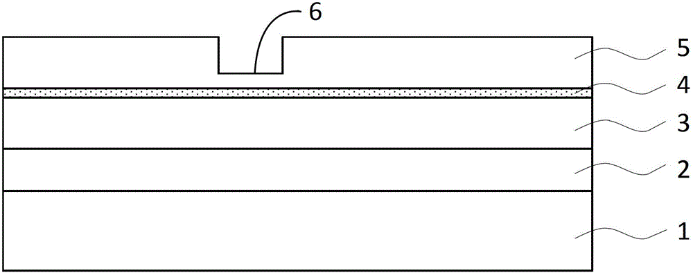
[0016] Embodiments of the present invention will be described below with reference to the drawings. Elements and features described in one drawing or one embodiment of the present invention may be combined with elements and features shown in one or more other drawings or embodiments. It should be noted that representation and description of components and processes that are not related to the present invention and known to those of ordinary skill in the art are omitted from the drawings and descriptions for the purpose of clarity.

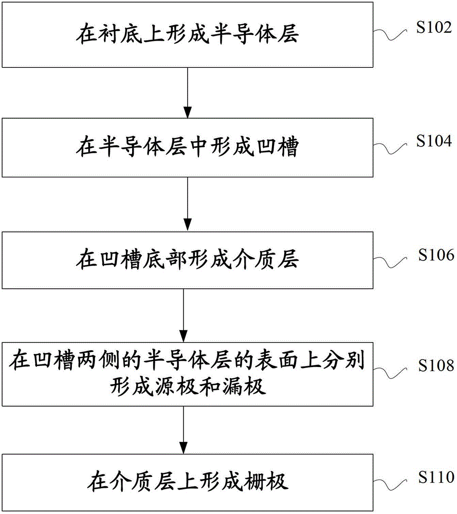
[0017] Refer below figure 1 , shows a flowchart of a method for manufacturing a high electron mobility transistor according to an embodiment of the present invention. A method of fabricating a high electron mobility transistor is provided, comprising:

[0018] Step S102, forming a semiconductor layer on the substrate;

[0019] Step S104, forming a groove in the semiconductor layer;

[0020] Step S106, forming a dielectric layer at the bottom of...


PUM


Abstract

The invention provides a high-electron mobility transistor and a manufacturing method for the same. The manufacturing method for the high-electron mobility transistor comprises the following steps: forming a semiconductor layer on a substrate; forming a groove in the semiconductor layer; forming a dielectric layer at the bottom of the groove; forming a source and a drain on the surface of the semiconductor layer; forming a gate on the dielectric layer. According to the high-electron mobility transistor and the manufacturing method for the same, the concentration of two-dimensional electron gas in a channel can be reduced, the forward threshold voltage of the high-electron mobility transistor can be increased, and the capability of a device in resisting noise interference can be enhanced.

Description

technical field [0001] The invention relates to the technical field of semiconductors, and in particular to a method for manufacturing a high electron mobility transistor. Background technique [0002] Traditional silicon technology has gradually reached its physical limit. Due to the large substrate leakage current, wide-bandgap semiconductor materials are better than semiconductors manufactured by traditional silicon processes in high-power and high-frequency circuits. As a third-generation semiconductor material, gallium nitride has the characteristics of large band gap, high breakdown voltage, high electron saturation mobility, small dielectric constant, strong radiation resistance and good chemical stability. , detection and high-temperature high-frequency circuits are widely used. The two-dimensional electron gas (2DEG) generated in the interface heterojunction of gallium nitride (GaN) and aluminum gallium nitride (AlGaN) has inherent advantages for the fabrication o...

Claims


Application Information

Patent Timeline
Patent Type & Authority Patents(China)
IPC IPC(8): H01L29/778H01L29/10H01L21/335
CPCH01L29/0684H01L29/1033H01L29/66462H01L29/7787
Inventor 包琦龙邓坚罗军赵超
Owner INST OF MICROELECTRONICS CHINESE ACAD OF SCI
Learn More