Mask plate and manufacture method of array base plate

一种阵列基板、制作方法的技术,应用在阵列基板的制作领域,能够解决显影速度和蚀刻速度慢、电阻变小、增大等问题,达到消除显示不均匀现象、减小电阻差的效果

Active Publication Date: 2013-09-25
TCL CHINA STAR OPTOELECTRONICS TECH CO LTD
View PDF8 Cites 4 Cited by
  • Summary
  • Abstract
  • Description
  • Claims
  • Application Information

AI Technical Summary

Problems solved by technology

The reason for this is that in the exposure step, the optical path is difficult to be completely collimated, there will be a small amount of side light, and the exposure area will be illuminated by both collimated light and side light, but for part A of (b) As far as the area is concerned, since the pattern of the fan-shaped lead wire is not irradiated with light, the three sides of the A area are surrounded, that is to say, there are three sides of the A area that cannot be irradiated with side light, while other exposure areas can be irradiated with collimated light and side light, so The photosensitivity of area A is weaker than that of other exposure areas, and the chemical reaction of photoresist is slower, which causes the development and etching speed of area A to be slower than that of other exposure areas during the subsequent development and etching steps, and finally fan out the bent part of the lead There is more area A, and the line width of the bent part of the fan-out lead increases, and the resistance decreases accordingly, resulting in a further increase in the resistance difference

Method used


Image

  • Mask plate and manufacture method of array base plate
  • Mask plate and manufacture method of array base plate
  • Mask plate and manufacture method of array base plate

Examples


Embodiment Construction

[0023] The following will clearly and completely describe the technical solutions in the embodiments of the present invention with reference to the accompanying drawings in the embodiments of the present invention. Obviously, the described embodiments are only some, not all, embodiments of the present invention. Based on the embodiments of the present invention, all other embodiments obtained by persons of ordinary skill in the art without making creative efforts belong to the protection scope of the present invention.

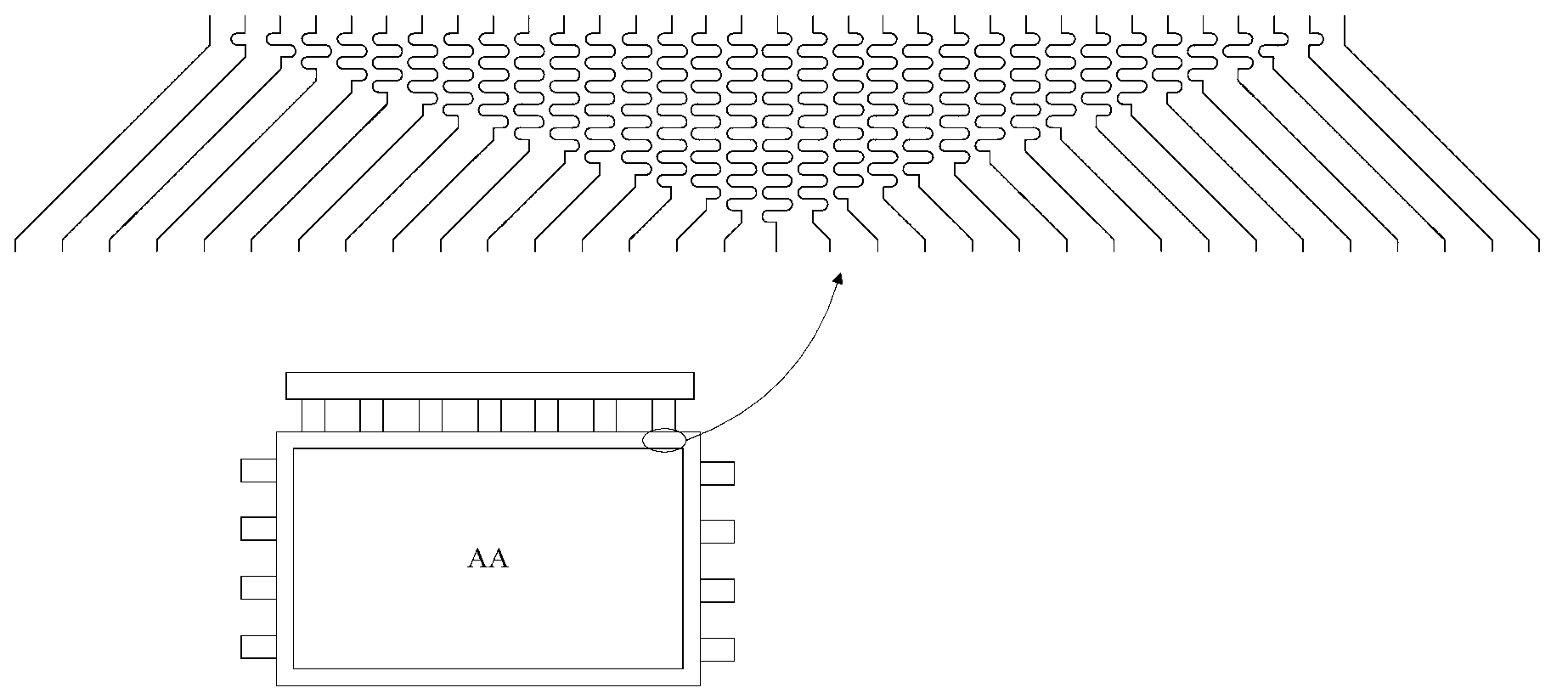
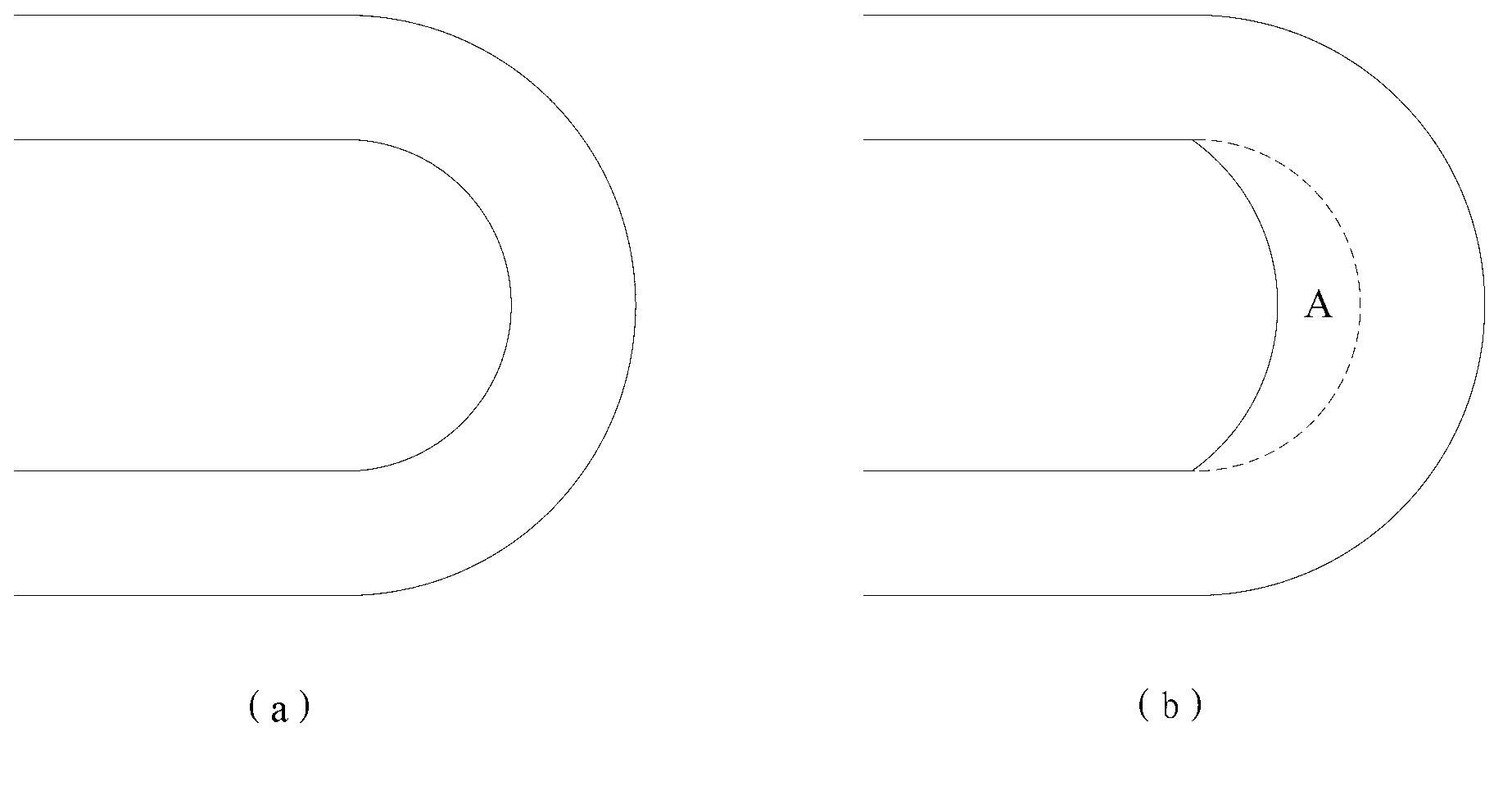
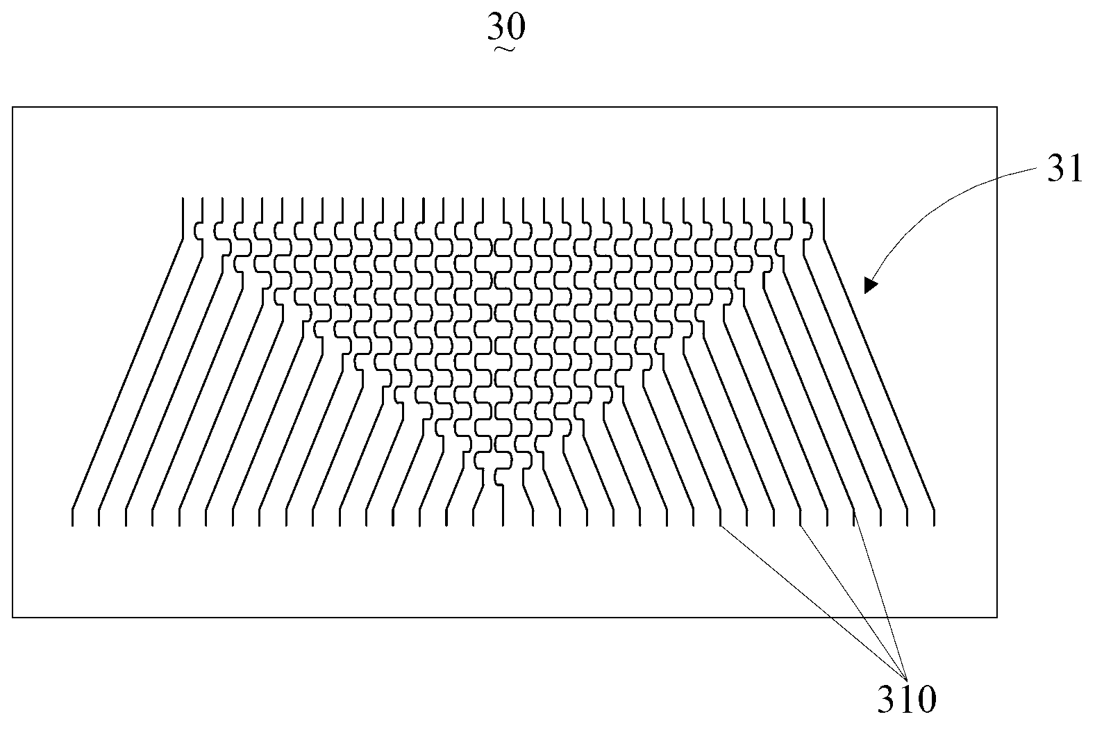
[0024] Please also refer to image 3 and Figure 4 , image 3 It is a structural schematic diagram of an embodiment of the mask plate of the present invention. Figure 4 yes image 3 A zoomed-in schematic of a fan-out die line on the mask shown.

[0025] The mask plate 30 is used for making fan-out leads in the non-active display area on the array substrate. The mask plate 30 includes a fan-out lead pattern 31, and the fan-out lead pattern 31 corresponds ...


PUM


Abstract

The invention discloses a mask plate and a manufacture method of an array base plate. The mask plate is used for manufacturing fan-out leads in an inefficient display area on the array base plate, and comprises fan-out lead patterns with a plurality of fan-out embossing die lines; each fan-out embossing die line has preset line width; at least part of the fan-out embossing die lines comprise at least one bending part; the line width of the bending part of a fan-out embossing die line is smaller than the preset line width of the identical fan-out embossing die line. According to the manufacture method, the mask plate is utilized to manufacture the array base plate. According to the invention, resistance differences among the fan-out leads can be reduced, and the phenomenon of uneven display can be eliminated.

Description

technical field [0001] The invention relates to the field of display manufacturing, in particular to a mask plate, and also to a method for manufacturing an array substrate. Background technique [0002] Display panels for manufacturing displays, including LCD (Liquid Crystal Display, Liquid Crystal Display) panels and OLED (Organic Light-Emitting Diode, Organic Light-Emitting Diode) panels, all need to form circuits through a photolithography process. [0003] The photolithography process mainly includes four steps of photoresist coating, exposure, photoresist development and etching. After the metal layer is formed on the glass substrate, photoresist coating is started to form a photoresist layer on the metal layer; then the photoresist layer is exposed; after the exposed photoresist layer is developed, the photoresist layer forms a pre- The designed circuit pattern; finally, the metal layer is etched, the metal without photoresist protection is etched away, and the remai...

Claims


Application Information

Patent Timeline
Patent Type & Authority Applications(China)
IPC IPC(8): G03F7/20G03F1/70H01L21/77
CPCG03F1/38G03F7/0007G03F1/00G03F1/70G03F7/20H01L27/1288H01L21/768H10K50/00
Inventor 郑华
Owner TCL CHINA STAR OPTOELECTRONICS TECH CO LTD
Why Eureka
Try Eureka