Encapsulating structure and encapsulating method for integrating acceleration sensor and magnetic sensor
An acceleration sensor, magnetic sensor technology, applied in the direction of electric solid device, semiconductor device, semiconductor/solid state device components, etc., can solve the problem of wasting PCB board space, reducing product assembly efficiency, increasing product cost, etc., to expand applications, The effect of packaging cost minimization
- Summary
- Abstract
- Description
- Claims
- Application Information
AI Technical Summary
Problems solved by technology
Method used
Image
Examples
no. 1 example 100
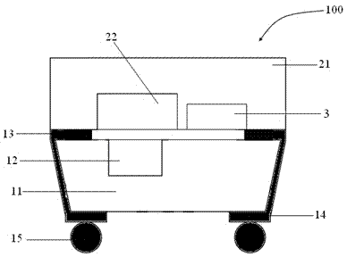
[0033] See figure 1 As shown, the present invention relates to a first embodiment 100 of a packaging structure integrating acceleration and magnetic sensors, which includes a first wafer 11 and a second wafer 21 .
[0034] Wherein the first wafer 11 is provided with a driving circuit for driving the acceleration sensor and a magnetic sensor and a structural circuit (not shown) of the acceleration sensor, and a first cavity 12 is also provided on the first wafer 11, and in the first cavity 12 A mechanical structure with an acceleration sensor. In addition, the front side of the first wafer 11 is provided with metal pads 13 outside the first cavity 12 .
[0035] The second wafer 21 is bonded on top of the first wafer 11 . A second cavity 22 for matching with the first cavity 12 is opened thereon, and the width of the second cavity 22 along the surface of the wafer is greater than or equal to the size of the mechanical mechanism of the acceleration sensor. The magnetic sensor ...
no. 2 example 200
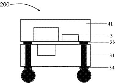
[0037] Further, such as figure 2 As shown, it illustrates the second embodiment 200 of the packaging structure of the integrated acceleration and magnetic sensor involved in the present invention, its structure is similar to that of the first embodiment, and also includes a first wafer 31 and a second wafer 41 . It differs from the first embodiment in that the metal pad 33 leads out the metal wire 34 in a different way, which is to drill a hole on the first wafer 31 and lead out through a through-silicon via (TSV) process, while the first embodiment The lead out of the pad in the example is realized by the sidewall lead process.
[0038] Further, such as image 3 As shown in -6, the present invention also provides a packaging method for manufacturing the integrated acceleration and magnetic sensor packaging structure involved in the present invention, which includes the following steps:
[0039] 1. First wafer and second wafer preparation and processing (such as image 3 ...
PUM
 Abstract
Description
Claims
Application Information
 - Generate Ideas
- Intellectual Property
- Life Sciences
- Materials
- Tech Scout
- Unparalleled Data Quality
- Higher Quality Content
- 60% Fewer Hallucinations
Browse by: Latest US Patents, China's latest patents, Technical Efficacy Thesaurus, Application Domain, Technology Topic, Popular Technical Reports.
© 2025 PatSnap. All rights reserved.Legal|Privacy policy|Modern Slavery Act Transparency Statement|Sitemap|About US| Contact US: help@patsnap.com


