Method for detecting atypical electronic components

A technology of electronic devices and detection methods, applied in the direction of electrical testing/monitoring, instruments, measuring electricity, etc., can solve the problems that are not enough to achieve zero defects, cannot guarantee the removal of devices, obstacles, etc.

Inactive Publication Date: 2012-03-21
IPPON INNOVATION
View PDF2 Cites 2 Cited by
  • Summary
  • Abstract
  • Description
  • Claims
  • Application Information

AI Technical Summary

Problems solved by technology

[0015] This shortcoming hinders: partly because it forces the manufacturer to resend the customer a new batch of replacement parts, thereby reducing the perceived quality level of the customer; Critical components in the operation of more complex systems, such as motor controllers or ABS braking systems
In this case, the failure of the device may cause a serious accident, and its consequences will far exceed the pure economic value of the device
[0016] The above risks drive manufacturers to choose to discard too many devices, including a large number of good devices, due to the use of univariate methods (PAT, etc.) or bivariate methods (regression, etc.) Manufacturer loses a few percent of yield and still cannot guarantee removal of potentially defective devices
[0017] Therefore, although effective, these methods are not sufficient to achieve zero defects

Method used


Image

  • Method for detecting atypical electronic components
  • Method for detecting atypical electronic components
  • Method for detecting atypical electronic components

Examples


Embodiment Construction

[0057] The invention is implemented by computer software executing on a microcomputer or other standard type of computer.

[0058] The present invention is intended to be used in the quality control of electronic device manufacture, and the specific opportunity of using the present invention is:

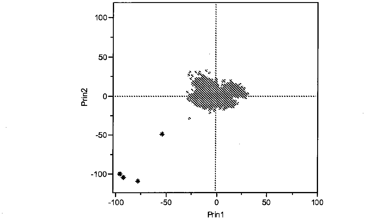
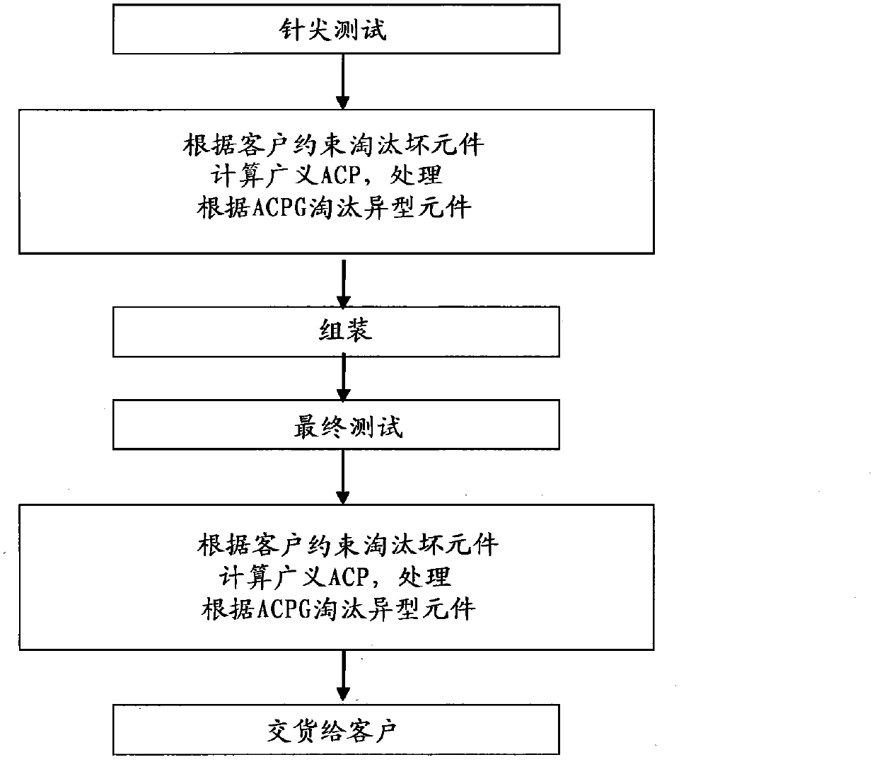
[0059] 1 / At the end of a needle-point (probe) test consisting of a plurality of electronic measurements and referred to as the first group of tests, i.e. at least one response to at least one test belonging to this first group of tests in the After the electronics outside the scope of the specification constraints have been discarded

[0060] 2 / Subsequently, at the end of the tests (second set of tests) performed after assembling the correct electronic device, ie the electronic device that has passed the pinpoint test and the test according to the method of the invention inside the enclosure.

[0061] The method according to the invention can be used in different ways after the fi...


PUM


Abstract

The invention relates to a method for detecting atypical electronic components for the quality control of n electronic components at the end of the manufacturing process, said components being subjected to a number p of unit tests providing digital data, said set of n components including electronic components having a response to each of the p unit tests that lies within predetermined limits particular to each of the p tests, wherein the method comprises using the multi-dimensional information of the p dimension responses of said n electronic components. The method uses a generalised principal component analysis for detecting atypical parts in the semiconductor field, or in the fields including modules assembled using electronic components (e.g. an ABS module, a smart card, etc.). The aim of the method is to get close to "zero defect", wherein no part is detected to be substandard by the client.

Description

technical field [0001] The invention relates to the field of quality control of components, especially electronic devices. Background technique [0002] The semiconductor industry produces integrated circuits, so-called electronic devices, which are fabricated on groups of silicon wafers, each wafer comprising hundreds of devices. [0003] In order to guarantee the functionality of these electronic devices, a first set of tests called needle-tip (or probe) tests are performed on the individual devices, which still form part of the wafer. [0004] The various tests, each consisting of electronic measurements, are combined with specification constraints determined especially for the target customers of these electronic components. [0005] If the electronic device's response to at least one test does not meet the specifications for that test in the first set of tests (probes), the electronic device is considered defective and is discarded when it is separated from the wafer. ...

Claims


Application Information

Patent Timeline
Patent Type & Authority Applications(China)
IPC IPC(8): G05B23/02
CPCG01R31/2894
Inventor 弗朗索瓦·贝热雷安娜·鲁伊斯卡罗勒·苏阿尔亨利·科西尼斯
Owner IPPON INNOVATION
Why Eureka
Try Eureka