Method and system for verifying timing sequence calibration function of dynamic random access memory (DRAM) controller
A technology of timing verification and verification method, applied in the field of electronics, can solve the problems of inability to test complete motherboards, different motherboards, and low coverage.
- Summary
- Abstract
- Description
- Claims
- Application Information
AI Technical Summary
Problems solved by technology
Method used
Image


Examples
Embodiment 1
[0039] figure 1 The method for verifying the timing verification function of the DRAM controller provided by Embodiment 1 of the present invention is shown, and the method includes the following steps:
[0040] In step S101, a static delay is performed according to a preset static delay value, and the static delay value is a random value or an ergodic value within a specified range.
[0041] In step S102, a test case transaction describing operations performed by the data transmission bus connected to the DRAM controller is generated.
[0042] In the embodiment of the present invention, the bus includes a register bus and a data transmission bus.
[0043] In the embodiment of the present invention, each test case transaction includes two parts, command and data, which are used to describe whether the operation of the bus is reading or writing, and the address for reading and writing.
[0044] In step S103, a control transaction is generated according to the above-mentioned t...
Embodiment 2
[0049] figure 2The method for verifying the timing verification function of the DRAM controller provided by Embodiment 2 of the present invention is shown, and the method includes the following steps:
[0050] In step S201, a preset static delay value is generated.
[0051] In step S202, a static delay is performed according to a preset static delay value, and the static delay value is a random value or an ergodic value within a specified range.
[0052] In step S203, start the timing verification operation of the DRAM controller, and monitor whether the timing verification operation is correctly completed.
[0053] In step S204, when the monitoring timing verification operation ends correctly, a test case transaction describing the operation performed by the data transmission bus connected to the DRAM controller is generated.
[0054] In step S205, a control transaction is generated according to the test case transaction, and the control transaction includes a command part...
Embodiment 3
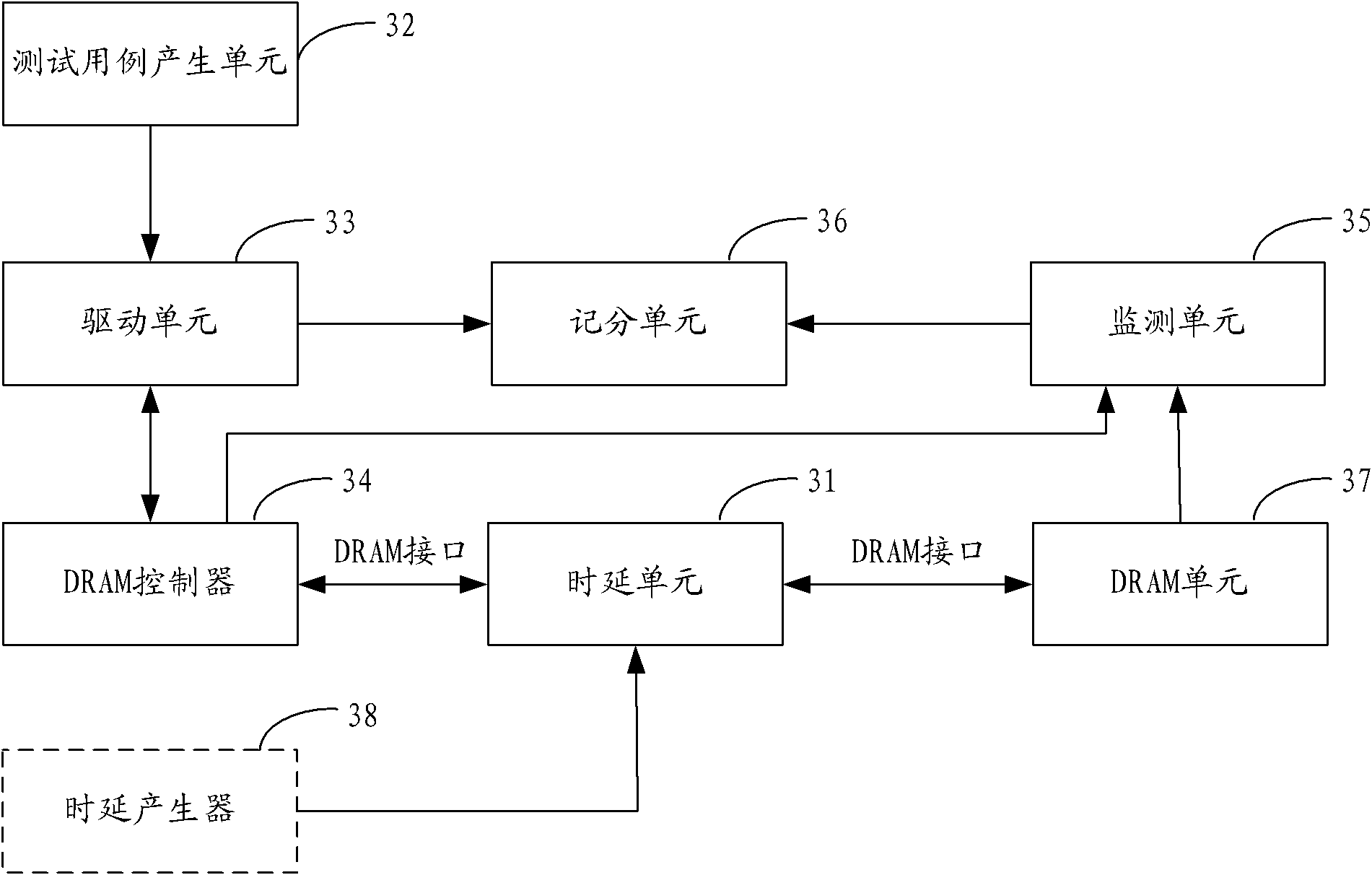
[0060] image 3 The verification system of the DRAM controller timing verification function provided by the embodiment of the present invention is shown, the system includes: a delay unit 31, a test case generation unit 32, a drive unit 33, a DRAM controller 34, a monitoring unit 35, and a scoring unit 36 and DRAM unit 37.
[0061] The delay unit 31 performs a static delay on the data line in the DRAM interface and each bit of the strobe pulse of the data line according to a preset static delay value, and the static delay value is a random value within a specified range or Iterate over the values.
[0062] The test case generation unit 32 generates a test case transaction describing operations performed by the data transfer bus connected to the DRAM controller 34 .
[0063] In the embodiment of the present invention, the drive unit 33 is connected to the DRAM controller 34 through a bus, and the bus includes a register bus and a data transmission bus.
[0064] In the embodi...
PUM
 Abstract
Description
Claims
Application Information
 - R&D
- Intellectual Property
- Life Sciences
- Materials
- Tech Scout
- Unparalleled Data Quality
- Higher Quality Content
- 60% Fewer Hallucinations
Browse by: Latest US Patents, China's latest patents, Technical Efficacy Thesaurus, Application Domain, Technology Topic, Popular Technical Reports.
© 2025 PatSnap. All rights reserved.Legal|Privacy policy|Modern Slavery Act Transparency Statement|Sitemap|About US| Contact US: help@patsnap.com