Eureka AIR delivers breakthrough ideas for toughest innovation challenges, trusted by R&D personnel around the world.

Process for manufacturing organic electroluminescent element, organic electroluminescent element, organic EL display, and organic EL lighting

A technology of electroluminescent element and manufacturing method, which is applied to the manufacturing of electroluminescent light sources, electrical components, semiconductor/solid-state devices, etc., to achieve the effects of high brightness and long driving life

Active Publication Date: 2012-02-08
MITSUBISHI RAYON CO LTD
View PDF23 Cites 6 Cited by
  • Summary
  • Abstract
  • Description
  • Claims
  • Application Information

AI Technical Summary

Problems solved by technology

[0004] For example, Patent Document 1 discloses that a composition containing anthracene derivatives and arylamine compounds is wet-formed to form a light-emitting layer, thereby producing a blue fluorescent device, but device characteristics such as driving life need to be improved

Method used

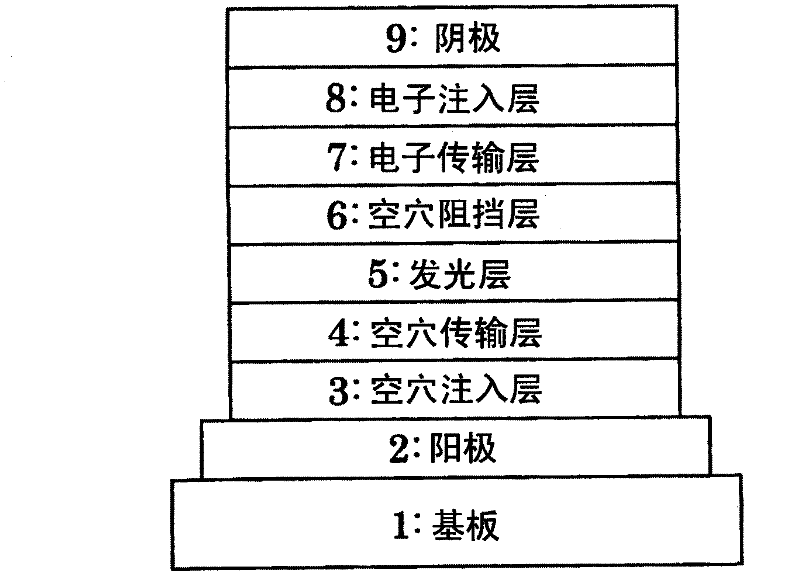

Image

  • Process for manufacturing organic electroluminescent element, organic electroluminescent element, organic EL display, and organic EL lighting
  • Process for manufacturing organic electroluminescent element, organic electroluminescent element, organic EL display, and organic EL lighting
  • Process for manufacturing organic electroluminescent element, organic electroluminescent element, organic EL display, and organic EL lighting

Examples


Embodiment

[0373] Next, although an Example demonstrates this invention more concretely, this invention is not limited to description of a following Example unless the summary is exceeded.

[0374] [Measurement of Relative Permittivity]

reference example 1

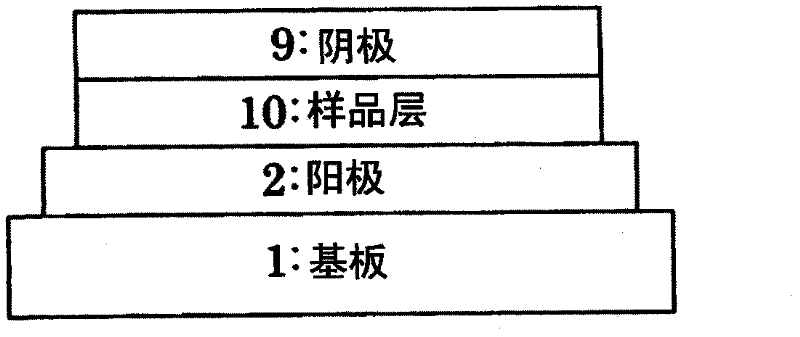
[0376] make figure 2 Device for measuring relative permittivity with the structure shown. A product obtained by depositing an indium tin oxide (ITO) transparent conductive film (manufactured by Sanyo Vacuum Industries Co., Ltd., manufactured by Sanyo Vacuum Industries Co., Ltd., by sputtering into film product) was patterned into stripes with a width of 2 mm to form electrodes 2 . The patterned ITO substrate was washed in the order of ultrasonic cleaning with aqueous surfactant solution, water washing with ultrapure water, ultrasonic cleaning with ultrapure water, and water washing with ultrapure water, and then dried with compressed air. Finally, ultraviolet ozone washing is carried out. This ITO functions as an electrode.

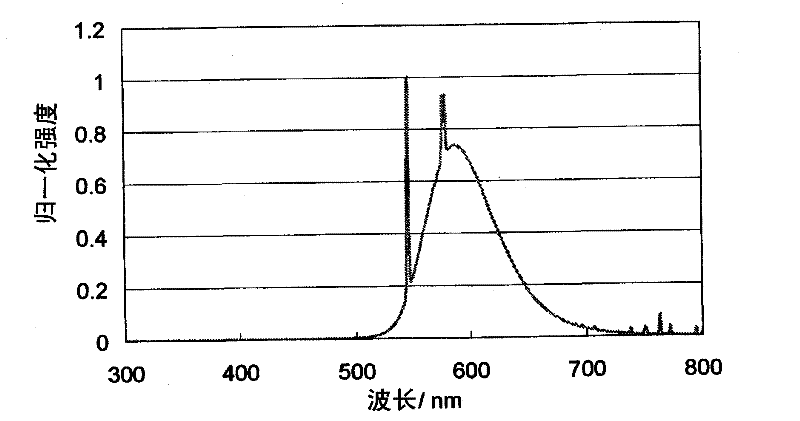
[0377] Preparation contains the compound (C1) shown in following structural formula, aromatic amine compound (C2) and the coating liquid of compound (D1), in image 3 In the environment of the spectrum shown, a film was formed on an ITO patterned sub...

reference example 2

[0397] In Reference Example 1, except for having Figure 4 An element for relative permittivity measurement was produced in the same manner as in Reference Example 1 except that the film-forming sample layer 10 was formed under the environment of the spectrum shown.

[0398] The obtained values ​​of relative permittivity are shown in Table 1.


PUM

PropertyMeasurementUnit
boiling pointaaaaaaaaaa
thicknessaaaaaaaaaa
boiling pointaaaaaaaaaa

Abstract

Disclosed is an organic electroluminescent element which has a light-emitting layer produced by a wet film formation method and containing an arylamine compound, and which has a long operation life. Also disclosed are an organic EL display and an organic EL lighting, each of which comprises the organic electroluminescent element. Further disclosed is a process for manufacturing an organic electroluminescent element which has a light-emitting layer produced by a wet film formation method and containing an arylamine compound, and which has a long operation life. The organic electroluminescent element is characterized by comprising a first electrode, a second electrode formed so as to face the first electrode, and a light-emitting layer intercalated between the first electrode and the second electrode, wherein the light-emitting layer is a layer containing an arylamine compound, and the light-emitting layer is formed by a wet film formation method under such conditions that a light having a wavelength shorter than 500 nm is blocked.

Description

technical field [0001] The present invention relates to a manufacturing method of an organic electroluminescent element, an organic electroluminescent element, an organic EL display and an organic EL lighting including the element. Background technique [0002] In recent years, the development of organic electroluminescent (organic EL) elements has been vigorously advanced as a technology for producing light-emitting devices such as displays and lighting, and practical use has begun mainly for small to medium-sized displays. This organic EL element emits light by injecting positive and negative charges (carriers) into an organic thin film sandwiched between electrodes, and recombining the carriers. [0003] The organic EL elements put into practical use at present are generally produced by the following method: heating a relatively low molecular weight compound under high vacuum conditions, and vapor-depositing it on a substrate arranged above. However, this vacuum vapor de...

Claims


Application Information

Patent Timeline
Patent Type & Authority Applications(China)
IPC IPC(8): H01L51/50C09K11/06H05B33/10
CPCC08G61/12C08G2261/3327C08G2261/512C08G2261/95C09K11/06C09K2211/1007C09K2211/1011C09K2211/1014H05B33/20C09B57/00C09B57/001C09B57/008H10K71/12H10K85/111H10K85/631H10K85/342H10K50/11H10K85/615
Inventor 冈部一毅
Owner MITSUBISHI RAYON CO LTD
Why Eureka
Eureka Blog
Learn More