Array antenna and method for manufacturing array antenna
A technology of array antennas and antenna elements, which is applied to antennas, individually powered antenna arrays, electrical components, etc., to achieve the effect of reducing useless radiation
- Summary
- Abstract
- Description
- Claims
- Application Information
AI Technical Summary
Problems solved by technology
Method used
Image
Examples
no. 1 approach
[0045] A first embodiment for carrying out the present invention will be described in detail with reference to the drawings.
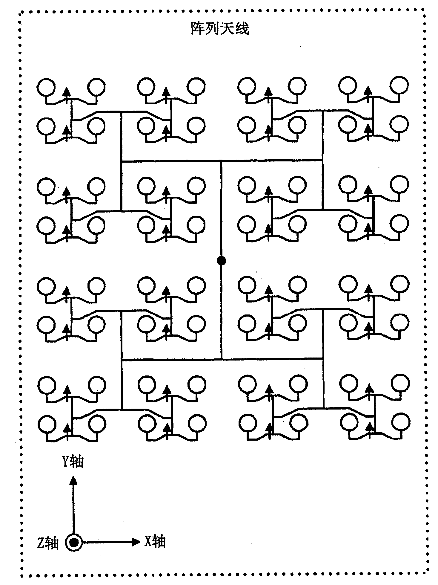
[0046] Figure 5 It is a circuit diagram showing the configuration of the array antenna 1 of this embodiment. Referring to this figure, array antenna 1 has a plurality of antenna elements A1, A2, etc., and a power supply circuit.
[0047] In this figure, an X-Y plane including an X-axis and a Y-axis is parallel to the paper surface, and a Z-axis is in a direction perpendicular to the X-Y plane. Moreover, all the antenna elements and the lines of the power supply circuit are arranged on the printed circuit board on the X-Y plane. For example, this Z-axis direction is set as the main lobe direction of the array antenna 1 .
[0048] In order to reduce the loss, the printed circuit board is suitable to use PTFE (Polytetrafluoroethylene) as the material, but for the purpose of reducing the material cost, BT (bismaleimide triazine, Bismaleimide-Triazine) ...
no. 2 approach
[0069] refer to Figure 9 A second embodiment of the present invention will be described. This figure is a circuit diagram showing the configuration of the array antenna 1a of this embodiment. Referring to this figure, the antenna elements and microstrip lines of this embodiment are divided into four groups (first to fourth subarrays).
[0070] If the offset of the second sub-array relative to the first sub-array is set to δ, then the offset of the third sub-array relative to the first sub-array is twice that of the fourth sub-array relative to the first sub-array. is offset by three times that.
[0071] If the offset of the second subarray relative to the first subarray and the offset of the fourth subarray relative to the first subarray are the same value, then the X coordinates of the unwanted radiation wave sources in the second and fourth subarrays Same, no offset. However, in this embodiment, the offsets of the sub-arrays other than the first sub-array relative to th...
no. 3 approach
[0073] refer to Figure 10 A third embodiment of the present invention will be described. This figure is a circuit diagram showing the configuration of the array antenna 1b of this embodiment. Referring to this figure, in the array antenna 1b, the sub-arrays are shifted in each column along the arrangement direction.
[0074] According to the configuration of the array antenna 1 of the first embodiment, if the offset is performed every two columns, the columns in each sub-array will not be offset. However, as shown in the configuration of the present embodiment, when offset is performed for each column, the sources of unwanted radiation of each column are dispersed, further degrading the side lobe characteristics.
PUM
 Abstract
Description
Claims
Application Information
 - R&D
- Intellectual Property
- Life Sciences
- Materials
- Tech Scout
- Unparalleled Data Quality
- Higher Quality Content
- 60% Fewer Hallucinations
Browse by: Latest US Patents, China's latest patents, Technical Efficacy Thesaurus, Application Domain, Technology Topic, Popular Technical Reports.
© 2025 PatSnap. All rights reserved.Legal|Privacy policy|Modern Slavery Act Transparency Statement|Sitemap|About US| Contact US: help@patsnap.com


