Sputtering device and sputtering method

A sputtering, sputtering gas technology, used in sputtering, ion implantation, vacuum evaporation, etc.

Inactive Publication Date: 2011-11-16
ULVAC INC
View PDF4 Cites 8 Cited by
  • Summary
  • Abstract
  • Description
  • Claims
  • Application Information

AI Technical Summary

Problems solved by technology

[0008] However, it has been found that using the device with the above-mentioned structure, when forming a protective film of Cu or Ta on the micropore, if it is formed by self-discharge sputtering in the internal space of the target, the The problem that the film formed by sputtered particles covers the opening of the top surface of the micropore and closes it

Method used


Image

  • Sputtering device and sputtering method
  • Sputtering device and sputtering method
  • Sputtering device and sputtering method

Examples


Embodiment Construction

[0028] Embodiment of the invention

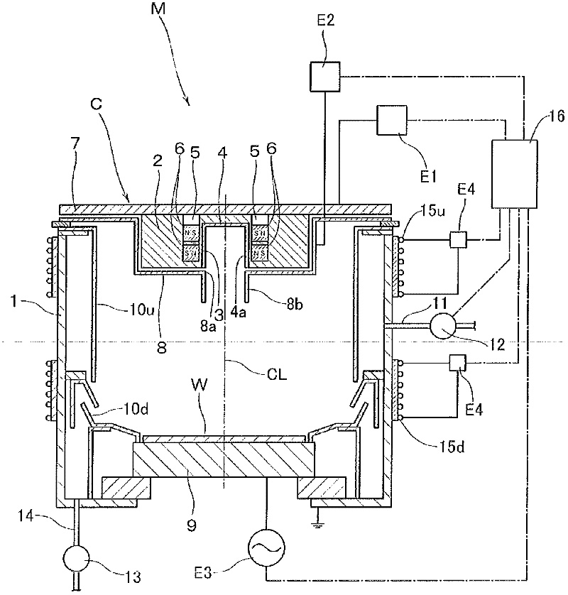
[0029] Hereinafter, with reference to the drawings, a sputtering apparatus having a cathode unit in an embodiment of the present invention will be described. Such as figure 1 As shown, the sputtering device M has a vacuum chamber 1 that can form a vacuum gas environment, and the top of the vacuum chamber 1 is equipped with a cathode unit C. In addition, in the following description, the top side of the vacuum chamber 1 is referred to as "upper", and the bottom side thereof is referred to as "lower" for description.

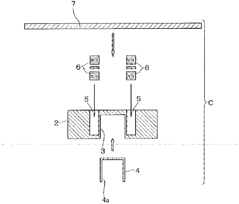
[0030] Such as figure 2 As shown, the cathode unit C has a cylindrical bracket 2 made of a conductive material, for example, the same material as the target material described later. A recess 3 is formed in the center of the lower surface of the bracket 2. The opening area of ​​the recess is set as The target 4 is inserted into the recess 3 within the range of

[0031] The target 4 selects a suitable material according to the com...


PUM


Abstract

Disclosed is a sputtering device capable of forming a film having good coverage with respect to each fine hole with a high aspect ratio formed the surface of a substrate. This device is equipped with: a vacuum chamber (1) in which a substrate (W) is disposed; a cathode unit (C), which is disposed in the vacuum chamber facing the substrate, and which has a holder (2) on one face of which at least one concave part (3) is formed, with a target material (4) having a closed-bottom cylindrical shape being mounted from the bottom side thereof, and to which is attached a magnetic field generation means (6) that generates a magnetic field in the interior space of the target material; an anode shield (8) to which a positive potential is applied; a gas introduction means (12) which introduces a sputter gas into the vacuum chamber; a power supply which supplies power to the cathode unit; a vertical magnetic field generation means comprised of a power supply and a coil (15) which is provided on the wall surface of the vacuum chamber around the reference axis connecting the cathode unit and the substrate; and a control means (16) which controls the on / off of the introduction of the sputter gas from the gas introduction means.

Description

Technical field [0001] The invention relates to a sputtering device and a sputtering method for forming a film on the surface of a substrate to be processed. Background technique [0002] In the film formation process of manufacturing semiconductor devices, for example, sputtering (hereinafter referred to as sputtering) equipment is used. As wiring patterns have become more and more refined in recent years, sputtering equipment for this purpose is required. On the entire surface of the micropores with high aspect ratio, the film can be formed with good coverage, that is, it is more required to improve the coverage effect. [0003] In the conventional sputtering device, a magnet assembly composed of a plurality of magnets with alternating polarity is installed behind the target (the side opposite to the sputtering surface), and the magnet assembly is in front of the target (the side of the sputtering surface). A tunnel-shaped magnetic field is generated, and the electron density in...

Claims


Application Information

Patent Timeline
Patent Type & Authority Applications(China)
IPC IPC(8): C23C14/34H01L21/285
CPCC23C14/3407C23C14/046H01J37/3447C23C14/351C23C14/358H01L21/2855H01J37/3405H01J37/3458H01J37/3452H01L21/02631
Inventor 森本直树滨口纯一
Owner ULVAC INC
Why Eureka
Try Eureka