Anti-floating and anti-tilt tool in circuit board wave soldering process

A wave soldering and circuit board technology, applied in the field of fixtures, can solve the problem of DIP parts floating, etc., to improve production efficiency, press stability, and reduce production costs.

Inactive Publication Date: 2011-10-19
昆山元崧电子科技有限公司
View PDF6 Cites 5 Cited by
  • Summary
  • Abstract
  • Description
  • Claims
  • Application Information

AI Technical Summary

Problems solved by technology

[0005] Aiming at the deficiencies existing in the prior art, the purpose of the present invention is to solve the floating height problem of DIP parts; to provide a circuit board wave soldering process anti-floating height and anti-tilt jig that saves manpower and working hours, improves efficiency, and stabilizes the pressing of DIP parts.

Method used


Image

  • Anti-floating and anti-tilt tool in circuit board wave soldering process
  • Anti-floating and anti-tilt tool in circuit board wave soldering process
  • Anti-floating and anti-tilt tool in circuit board wave soldering process

Examples


Embodiment Construction

[0015] In order to make the technical means, creative features, goals and effects achieved by the present invention easy to understand, the present invention will be further described below in conjunction with specific embodiments.

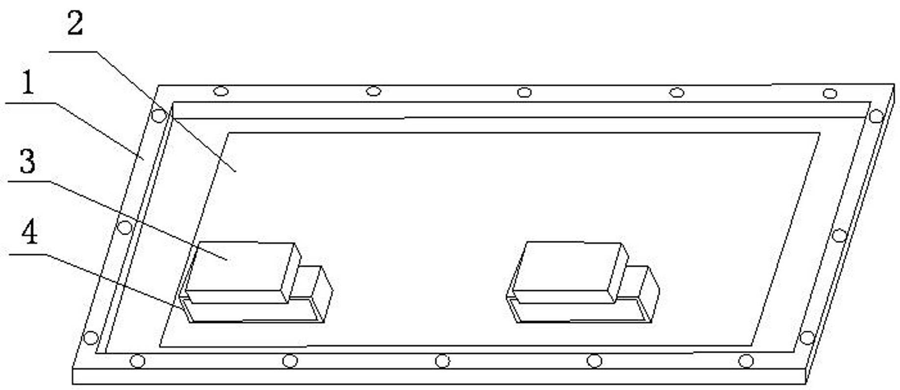
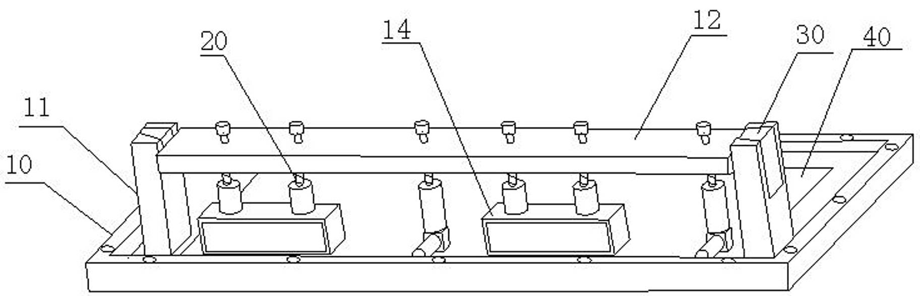
[0016] see figure 2 , the circuit board wave soldering process anti-floating height anti-tilt jig of the present invention includes a wave soldering carrier body 10, a PCB board 40 is placed in the wave soldering carrier body 10, and the wave soldering carrier body 10 is equipped with a device for pressing DIP A pressing device for parts, the pressing device includes a fixing frame 11 fixed on the wave soldering carrier body 10, a bead 12 arranged on the fixing frame 11, and a plurality of pressing member mechanisms 20 arranged on the bead 12, the pressing device of this embodiment There are six piece mechanism 20, and the number of piece piece mechanism 20 is set according to the number of DIP parts of PCB board 40.

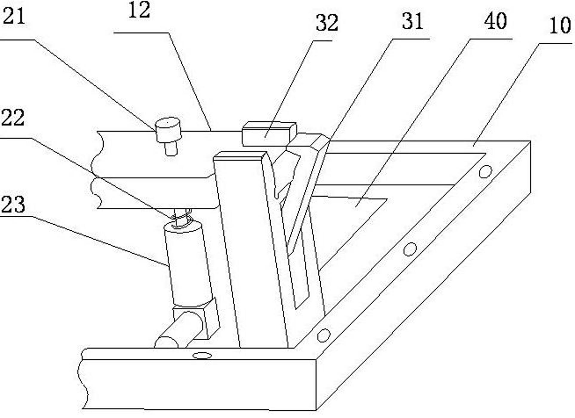
[0017] see image 3 , in ...


PUM


Abstract

The invention relates to an anti-floating and anti-tilt tool in a circuit board wave soldering process. The anti-floating and anti-tilt tool comprises a wave soldering tool supporter used for placing PCB (Printed circuit board). The invention is characterized in that the wave soldering tool supporter is provided with a press apparatus used for pressing DIP components, the press apparatus comprises a fixed mount arranged in the wave soldering tool supporter, a press strip and a plurality of press mechanisms arranged on the press strip, and the two ends of the press strip is fixed on the fixed mount through a clamp mechanism. When the DIP components pass across a furnace, each DIP component is pressed by the press mechanisms to prevent the problems of skew of components and high floating ofthe DIP components caused by that tin blocks fall off by the vibration of the wave soldering tool supporter in a wave soldering track in the transmission process. The anti-floating and anti-tilt toolin circuit board wave soldering process provided in the invention has the advantages of saving manpower, raising production efficiency and stabilizing the DIP components. Thus the enterprise production cost is reduced.

Description

technical field [0001] The invention relates to a jig, in particular to an anti-floating height and anti-tilt jig for a circuit board wave soldering process. Background technique [0002] In the wave soldering process, for the problem of the floating height of the DIP parts of the PCB board, the pressing method currently used in the market is to press the parts with tin blocks, such as figure 1 As shown, the PCB board 2 is placed on the wave soldering fixture 1, and the DIP part 4 is pressed on the PCB board 2 through the tin block 3. Due to the high risk of this pressing method: [0003] 1. The tin block 3 passes through the furnace on the DIP part 4, without any fixing method, it is fixed entirely by its own weight and friction. Moreover, the wave soldering fixture 1 vibrates during the transmission process on the wave soldering track, and the tin block 3 is easy to drop, which not only causes the DIP part 4 to float high, but also causes other parts to be skewed when the...

Claims


Application Information

Patent Timeline
IPC IPC(8): H05K3/34
Inventor 陈松
Owner 昆山元崧电子科技有限公司
Why Eureka
Try Eureka