
Nano-scale three-dimensional shape measurement method based on scanning electron microscope

A technology of scanning electron microscopy and three-dimensional topography, which is applied in the field of precision measurement, can solve the problems of time drift, limited value, and the inability to eliminate the influence of time drift measurement accuracy, and achieve the effect of simple operation

Active Publication Date: 2012-12-19
HUAZHONG UNIV OF SCI & TECH
View PDF0 Cites 0 Cited by
  • Summary
  • Abstract
  • Description
  • Claims
  • Application Information

AI Technical Summary

Problems solved by technology

The research results show that the non-parametric distortion correction method adopted by this method is better than the parametric distortion correction method commonly used in the macroscopic field, and better calibration results can be obtained at lower magnifications, but at high magnifications There are still significant measurement errors
The main reason for this phenomenon is that the shooting process of electronic images is different from that of optical images, and the scanning process of electron beams is controlled by electromagnetic fields (similar to the lenses in optical imaging systems). Even in the most advanced SEM systems at present, the electronic The deflection of the beam is still an open-loop system (that is, its actual deflection parameters or positions are uncontrollable), and the scanning process is affected by factors such as electromagnetic field fluctuations, time drift during scanning, electron beam position changes, thermal changes on the sample surface, and mechanical vibrations. Combined effects, the captured electronic image not only has obvious spatial distortion, but also produces complex time drift with random characteristics (Time Drift)
In 2006, M.A. Sutton et al. conducted a preliminary analysis of the reasons for the time drift of electronic images, and proved through experiments that the existing calibration algorithms cannot eliminate the impact of time drift on measurement accuracy.
Relevant research institutes at home and abroad have made some progress in this area. However, since SEM was originally designed as an observation tool, it is not used for measurement. If you want to combine it with digital photogrammetry methods to form an effective high-precision The three-dimensional reconstruction method of micro-nano structure still has the following two main problems: 1) Since the imaging process of electronic images is different from that of traditional optical imaging systems, the captured electronic images have very serious spatial distortion and time drift. The impact of time drift on measurement accuracy cannot be eliminated; 2) There are still large differences in the mathematical model of the electronic imaging system, and the imaging model of the electronic imaging system cannot be correctly recognized, which affects the 3D reconstruction accuracy of micro-nano structures
Thus previous technical approaches are of limited value

Method used


Image

  • Nano-scale three-dimensional shape measurement method based on scanning electron microscope
  • Nano-scale three-dimensional shape measurement method based on scanning electron microscope
  • Nano-scale three-dimensional shape measurement method based on scanning electron microscope

Examples


Embodiment Construction

[0022] The present invention will be described in further detail below in conjunction with the accompanying drawings and examples.

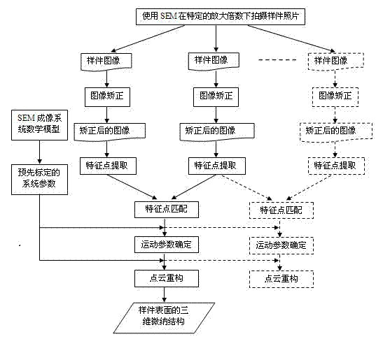
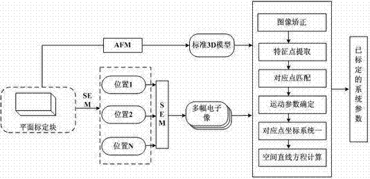
[0023] The workflow of the nanoscale three-dimensional shape measurement method based on the scanning electron microscope is as follows: use the scanning electron microscope imaging system to photograph the sample from at least two angles under the same magnification, and obtain a set of electronic images; use the digital image correlation method, For example, the Harris Detector method extracts feature point sets from multiple electronic images, and performs feature point matching to find out the corresponding points of the features; then uses the homograph matrix (Homograph) to determine the relative positional relationship of multiple images when they are taken , that is, the external parameters; finally, three-dimensional reconstruction is carried out according to the found feature corresponding points, external parameters and pre-calibrated s...


PUM


Abstract

The invention discloses a nano-scale three-dimensional shape measurement method based on a scanning electron microscope. The scanning electron microscope currently widely used is organically combined with the digital photogrammetry in macrocosmic measurement, the characteristics that the scanning electron microscope is easy to operate and can be used to take two-dimensional pictures with high amplification factor and large depth of field are fully utilized, and the advantage that digital photogrammetry can be used to automatically and precisely reconstruct the complete three-dimensional data of the surface of an measured object from the pictures taken from multiple angles is fully exerted. A group of sample pictures is obtained by using the scanning electron microscope to take sample pictures from multiple angles at the same amplification factor, the distortion of the pictures are corrected, the corrected pictures are reconstructed by using the digital picture correlation algorithm, and the complete three-dimensional point cloud data of the sample surface is reconstructed on the basis of the corrected pictures and pre-calibrated system parameters, thus the dense point cloud data of three-dimensional shape in the local range of a sample is measured accurately at the nano scale, and the three-dimensional measurement of the shape of a nano-scale micro device is realized.

Description

technical field [0001] The invention belongs to the field of precision measurement, and in particular relates to a nanoscale three-dimensional shape measurement method based on a scanning electron microscope. Background technique [0002] With the rapid development of Micro / Nano Electro Mechanical System (MEMS / NEMS), various micro / nano-scale microdevices are emerging, such as microgears, micronozzles, microsteps, etc., in order to ensure that these micro The processing quality of the device needs to be accurately measured. The geometric dimensions of these micro-devices are almost at the micro / nano scale, which cannot be measured by conventional methods. Therefore, it is very important to develop high-precision measurement methods and technologies at the nanoscale. [0003] The three-dimensional shape measurement method of micro-nano structure formed by combining the electronic image taken by scanning electron microscope (Scanning Electron Microscope, SEM) with the digital ...

Claims


Application Information

Patent Timeline
Patent Type & Authority Patents(China)
IPC IPC(8): G01B7/28
Inventor 史玉升李中伟王从军钟凯周钢朱晓鹏湛承诚
Owner HUAZHONG UNIV OF SCI & TECH
Learn More