Eureka AIR delivers breakthrough ideas for toughest innovation challenges, trusted by R&D personnel around the world.

Method for improving picture quality of GIP (Gate-in-Panel) liquid crystal display panel

A liquid crystal display panel and liquid crystal panel technology, which are applied in the field of liquid crystal display driving and improving the image quality of GIP liquid crystal display panels, can solve the problems such as the deterioration of the image quality of the after-image guide after shutdown, and achieve the improvement of after-image, image quality, and image quality improvement. Effect

Inactive Publication Date: 2011-02-09
NANJING CEC PANDA LCD TECH
View PDF5 Cites 3 Cited by
  • Summary
  • Abstract
  • Description
  • Claims
  • Application Information

AI Technical Summary

Problems solved by technology

[0007] The purpose of the present invention is to solve the problem that the picture quality of the afterimage after shutdown is reduced in the pixel of the existing liquid crystal display, and to invent a method that can eliminate the afterimage after the shutdown in time and improve the picture quality.

Method used


Image

  • Method for improving picture quality of GIP (Gate-in-Panel) liquid crystal display panel
  • Method for improving picture quality of GIP (Gate-in-Panel) liquid crystal display panel
  • Method for improving picture quality of GIP (Gate-in-Panel) liquid crystal display panel

Examples


Embodiment Construction

[0021] The present invention will be further described below in conjunction with the accompanying drawings and embodiments.

[0022] Such as Figure 4-7 shown.

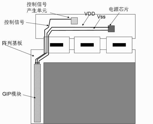
[0023] A method for improving the image quality of a GIP liquid crystal display panel, which adds a switching switch between the TFT on-voltage VDD and the TFT off-voltage Vss provided to the GIP unit by the printed circuit board, so that the voltage of VDD is switched when the liquid crystal panel is shut down On the line to Vss, input to the GIP unit, so that each scanning line outputs the TFT open voltage VDD, so that the Vss voltage is equal to the VDD voltage, and input to each SR unit through the array substrate to neutralize the voltage of the pixel , so as to achieve the purpose of eliminating the afterimage after shutdown, and improve the display quality of the GIP liquid crystal display panel.

[0024] Such as Figure 4 Shown, the present invention is in prior art ( image 3 ) on the basis of adding a sw...


PUM


Abstract

The invention relates to a method for improving the picture quality of a GIP (Gate-in-Panel) liquid crystal display panel, which is characterized in that a changeover switch is additionally arranged between a TFT (Thin Film Transistor) power-on voltage VDD and a TFT power-off voltage Vss of a GIP unit on a printed circuit board, so that the voltage of VDD is switched to a conducting wire of Vss and is output to the GIP unit when the liquid crystal display panel is powered off, and each scan line outputs the TFT power-on voltage VDD, the Vss voltage is equal to the VDD voltage and is input to each SR (Scanning Radiometer) unit through an array substrate to neutralize the voltage of pixels. The voltage value supplied to the conducting wire of Vss is switched to VDD by controlling the switch unit between VDD and Vss, so that the voltages input to all scan lines during power-off are VDD to turn on all TFT, and the purpose of improving a residual image is achieved without changing the design of the array substrate.

Description

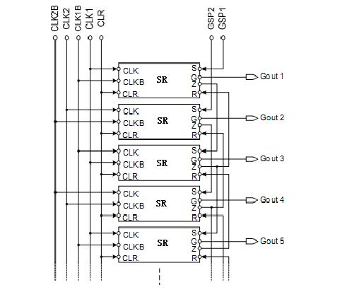
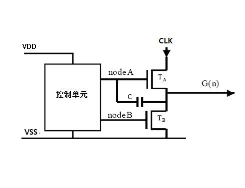
technical field [0001] The invention relates to a liquid crystal display technology, in particular to a liquid crystal display driving technology, in particular to a method for improving the image quality of a GIP liquid crystal display panel. Background technique [0002] At present, GIP (Gate In Panel) is a technology that integrates scanning chips on TFT-LCD panels, which can save scanning chips and reduce the cost of LCD panels. Each scan line corresponds to a shift register SR (Shift Register) unit; for example figure 1 shown. [0003] For each shift register SR unit, its basic architecture is as follows figure 2 Shown: It includes a pull-up unit and a pull-down unit. The function of the pull-up unit is to output VDD voltage to the scan line G(n) when the TFT TA is turned on, and drive the scan line to turn on the TFT on the scan line; the function of the pull-down unit is When the TFT TB is turned on, the TFT off voltage Vss is output to G(n) to turn off the TFT on...

Claims


Application Information

Patent Timeline
Patent Type & Authority Applications(China)
IPC IPC(8): G09G3/36
Inventor 王志军
Owner NANJING CEC PANDA LCD TECH
Why Eureka
Eureka Blog
Learn More