Imaging lens, imaging device and portable terminal
一种摄像透镜、透镜的技术,应用在便携终端,摄像装置领域,能够解决畸变大等问题,达到畸变小、传感入射角度小、良好像差性能的效果
- Summary
- Abstract
- Description
- Claims
- Application Information
AI Technical Summary
Problems solved by technology
Method used
Image

Examples
Embodiment approach 2
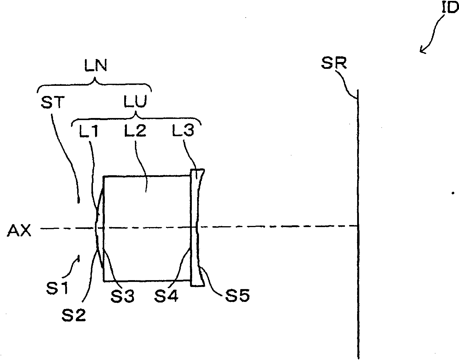
[0081] In the imaging device ID of Embodiment 2, the lens unit LU of the imaging lens LN of Reference Embodiment 1 is constituted by a cemented lens composed of three lens portions. Specifically, the lens unit LU is composed of the first lens L1, the second lens L2, and the third lens L3 from the object side, and has positive power as a whole. The first lens L1 is a plano-convex lens with a convex surface facing the object, and is formed of, for example, resin. The second lens L2 is a parallel flat plate and is formed of, for example, glass. The third lens L3 is a plano-concave lens whose concave surface faces the image, and is formed of, for example, resin. The first lens L1 and the second lens L2 are bonded directly or indirectly, and the second lens L2 and the third lens L3 are bonded directly or indirectly. Indirect bonding means, for example, bonding with an adhesive layer in between, and bonding with an optically functional film such as an infrared shielding filter in ...
Embodiment approach 12
[0087] In the imaging device ID of the twelfth embodiment, the aperture stop ST of the eighth to eleventh embodiments is positioned on the interface between the first lens L1 and the second lens L2. Therefore, the first lens L1 and the second lens L2 are indirectly bonded via the aperture stop ST. That is, the imaging lens LN of the twelfth embodiment has a structure in which the first lens L1, the aperture stop ST, the second lens L2, the third lens L3, and the parallel plane plate PT are arranged in order from the object side.
[0088] Next, the imaging lens LN referring to the imaging device IDs of Embodiments 1 and 3 to 7 and the imaging device IDs of Embodiments 2 and 8 to 12 will be described in detail.
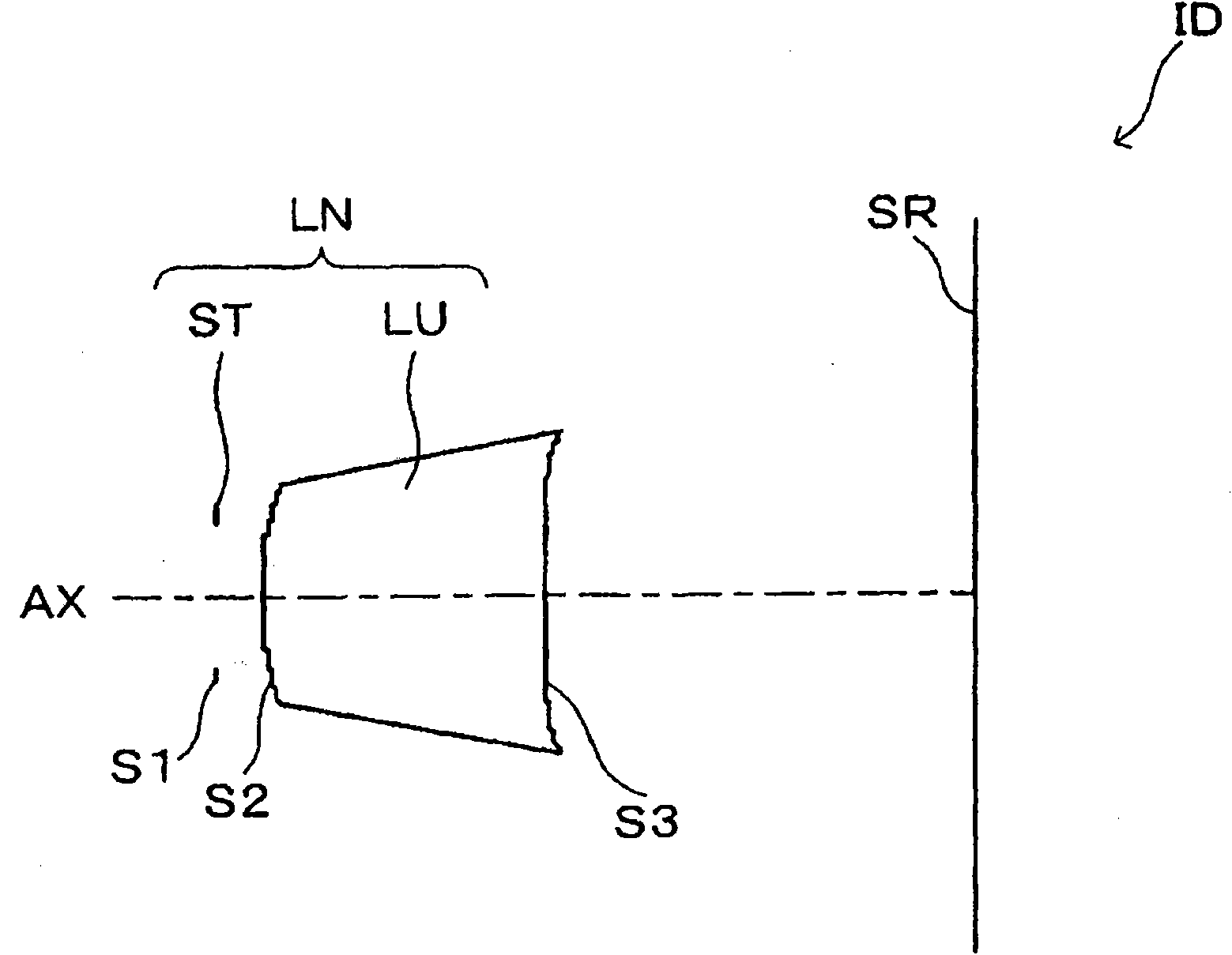
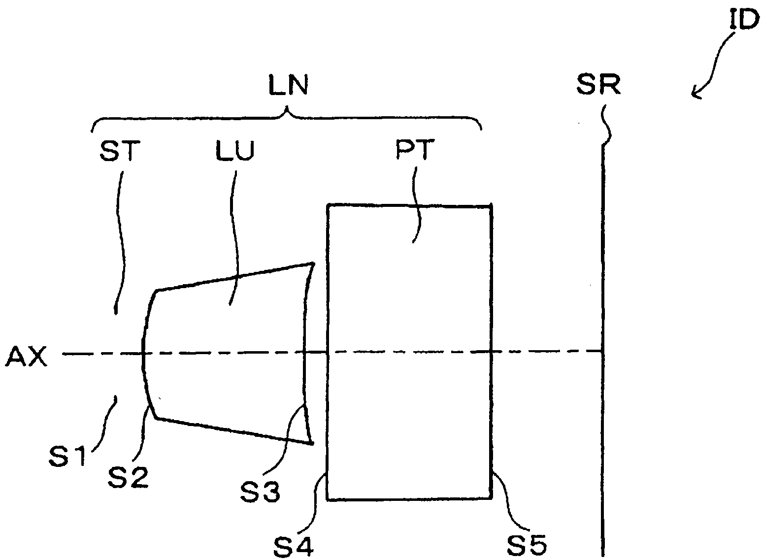
[0089] As described above, the imaging lens LN of each reference mode and embodiment includes an aperture stop ST and an optical element having a power consisting of one lens unit LU having a positive power. This lens unit LU may be composed of a single lens or may be ...
Embodiment
[0155] Next, as Reference Examples 1, 3 to 7 and Examples 2, 8 to 12, using configuration data, etc., the specific structures, etc. illustrate. Reference example 1, 3~7 and embodiment 2, 8~12 are numerical examples corresponding to above-mentioned each reference mode 1, 3~7 and implementation mode 2, 8~12 respectively, and each reference mode 1, 3~7 and Optical configuration diagrams of Embodiments 2, 8-12 ( figure 1 , 3 ~7 and figure 2 , 8 ˜12) represent the lens structures of the corresponding Reference Examples 1, 3-7 and Examples 2, 8-12, respectively.
[0156] In the compositional data of each reference example and working example, from the column on the left, the surface number Si, the radius of curvature r (mm), the distance on the axis d (mm), the refractive index nd to the d-line, and the refractive index to the d-line are shown in order. Abbe number vd. The surface number Si indicates the i-th surface from the object side. The surface with "*" on the surface ...
PUM
 Abstract
Description
Claims
Application Information
 - Generate Ideas
- Intellectual Property
- Life Sciences
- Materials
- Tech Scout
- Unparalleled Data Quality
- Higher Quality Content
- 60% Fewer Hallucinations
Browse by: Latest US Patents, China's latest patents, Technical Efficacy Thesaurus, Application Domain, Technology Topic, Popular Technical Reports.
© 2025 PatSnap. All rights reserved.Legal|Privacy policy|Modern Slavery Act Transparency Statement|Sitemap|About US| Contact US: help@patsnap.com