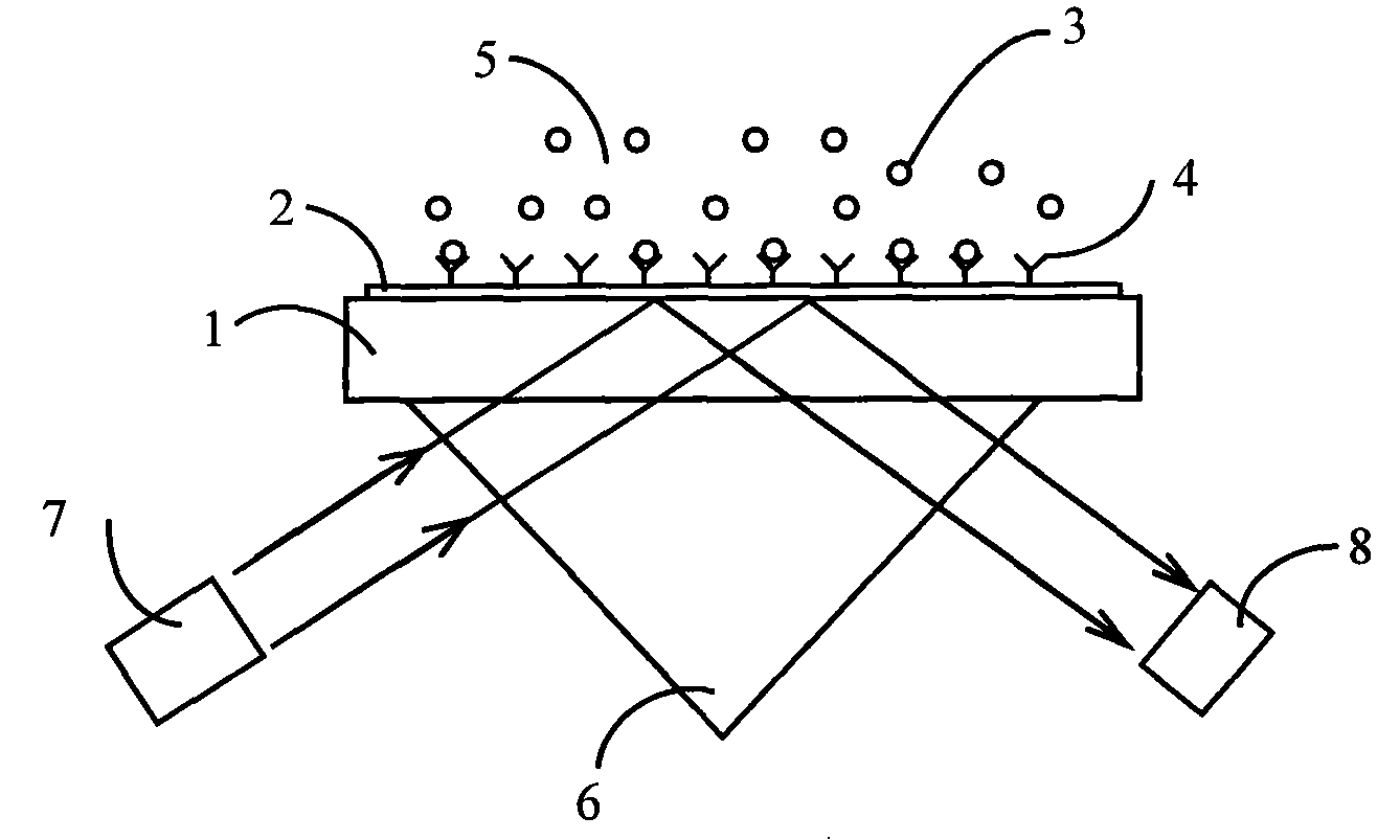
Waveguide coupling metal photonic crystal biosensor and detecting method thereof
A metal photonic crystal, biosensor technology, applied in instruments, measuring devices, scientific instruments, etc., can solve the problems of complex structure, high cost, and complicated system operation of biosensor devices.
- Summary
- Abstract
- Description
- Claims
- Application Information
AI Technical Summary
Problems solved by technology
Method used
Image
Examples
Embodiment 1
[0097] This embodiment is a front transmissive waveguide coupling one-dimensional metal photonic crystal biosensor and its detection method:
[0098] The substrate 21 used in this embodiment is made of glass with thickness D=1mm, and the waveguide layer 22 is made of indium tin oxide (ITO) thin film glass sheet with thickness d=200nm.
[0099] In this embodiment, a one-dimensional gold photonic crystal with a period of Λ=330nm is prepared on the ITO waveguide layer of a glass substrate by a preparation method of interference lithography combined with a solution method, and a waveguide-coupled one-dimensional gold photonic crystal biosensor is obtained. When using this sensor for detection, the detection method is as follows:
[0100] 1) A receptor (antibody) 4 with a specific recognition function for the ligand (antigen) 3 is immobilized on the surface of the metal photonic crystal 23 in the waveguide-coupled one-dimensional metal photonic crystal biosensor to form the initial...
Embodiment 2
[0106] This embodiment is a back transmission type two-dimensional waveguide coupling metal photonic crystal biosensor and its detection method:
[0107] The substrate used in this embodiment is glass with a thickness of D=1mm, and the waveguide layer is made of ITO glass sheet with a thickness of d=200nm.
[0108] In this example, two-dimensional gold photonic crystals with Λ=350nm period in both directions were prepared on the ITO waveguide layer of the glass substrate by the preparation method of interference lithography combined with the solution method, and a waveguide-coupled two-dimensional gold photonic crystal biosensor was obtained. When using this sensor for detection, the detection method is as follows:
[0109] 1) Immobilize the receptor (antibody) 4 that has a specific recognition function for the ligand (antigen) 3 on the surface of the metal photonic crystal in the two-dimensional waveguide-coupled metal photonic crystal biosensor to form the initial diaphragm ...
Embodiment 3
[0115] This embodiment is a front reflective waveguide coupling one-dimensional metal photonic crystal biosensor and its detection method:
[0116] The substrate used in this embodiment is glass with a thickness of D = 1 mm, and the waveguide layer is an ITO glass sheet with a thickness of d = 210 nm.
[0117] In this embodiment, a one-dimensional gold photonic crystal with a period of Λ=400nm is prepared on an ITO waveguide of a glass substrate by a preparation method of interference lithography combined with a solution method, and a waveguide-coupled one-dimensional gold photonic crystal biosensor is obtained;
[0118] 1) Immobilize the antibody with specific recognition function on the antigen on the surface of the metal photonic crystal in the waveguide-coupled one-dimensional metal photonic crystal biosensor to form the initial diaphragm of the sensor, and contact the blank sample solution with the surface of the metal photonic crystal 23 ;
[0119] 2) The spectral test ...
PUM
| Property | Measurement | Unit |
|---|---|---|
| thickness | aaaaa | aaaaa |
| thickness | aaaaa | aaaaa |
| thickness | aaaaa | aaaaa |
Abstract
Description
Claims
Application Information
 - R&D
- Intellectual Property
- Life Sciences
- Materials
- Tech Scout
- Unparalleled Data Quality
- Higher Quality Content
- 60% Fewer Hallucinations
Browse by: Latest US Patents, China's latest patents, Technical Efficacy Thesaurus, Application Domain, Technology Topic, Popular Technical Reports.
© 2025 PatSnap. All rights reserved.Legal|Privacy policy|Modern Slavery Act Transparency Statement|Sitemap|About US| Contact US: help@patsnap.com


