Detection method for silicon wafer warpage degree

A detection method and wafer technology, applied in the detection of whether the warpage degree of the wafer will affect the subsequent process, the detection process field, can solve the problem of not being able to detect the uniformity of the wafer warpage, and achieve the effect of eliminating position anomalies

Inactive Publication Date: 2009-05-27
SEMICON MFG INT (SHANGHAI) CORP
View PDF0 Cites 23 Cited by
  • Summary
  • Abstract
  • Description
  • Claims
  • Application Information

AI Technical Summary

Problems solved by technology

That is to say, the existing inspection method cannot detect whether the warpage of the wafer is uniform

Method used


Image

  • Detection method for silicon wafer warpage degree
  • Detection method for silicon wafer warpage degree
  • Detection method for silicon wafer warpage degree

Examples


Embodiment Construction

[0011] The preferred embodiments of the method for detecting the degree of wafer warpage provided by the present invention will be described in detail below in conjunction with the accompanying drawings, in order to further understand the technical solution, purpose and beneficial effects of the invention. The present invention can be applied in any process, but in this embodiment, the process of the wafer is a thermal oxidation step for forming an oxide film on the surface of the wafer.

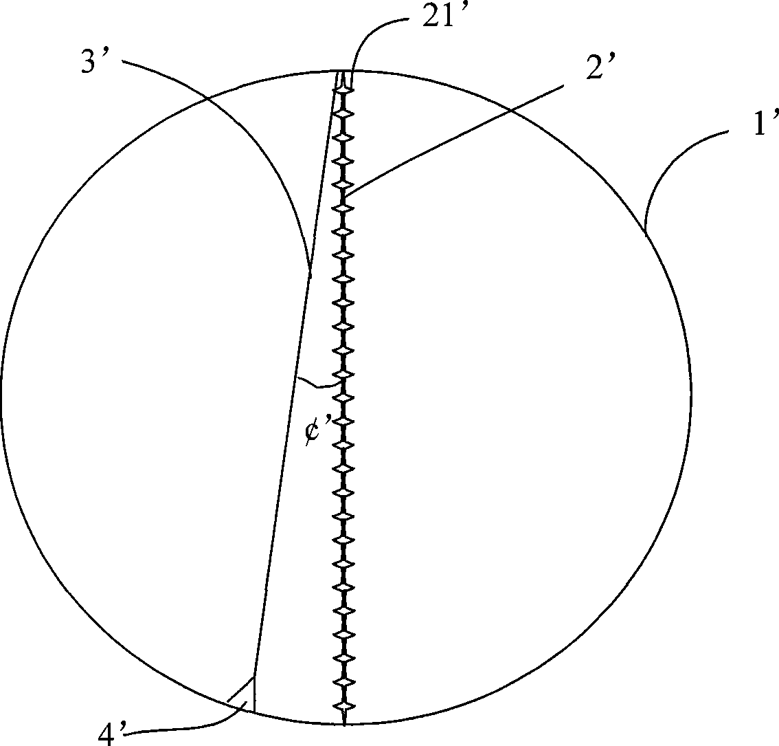
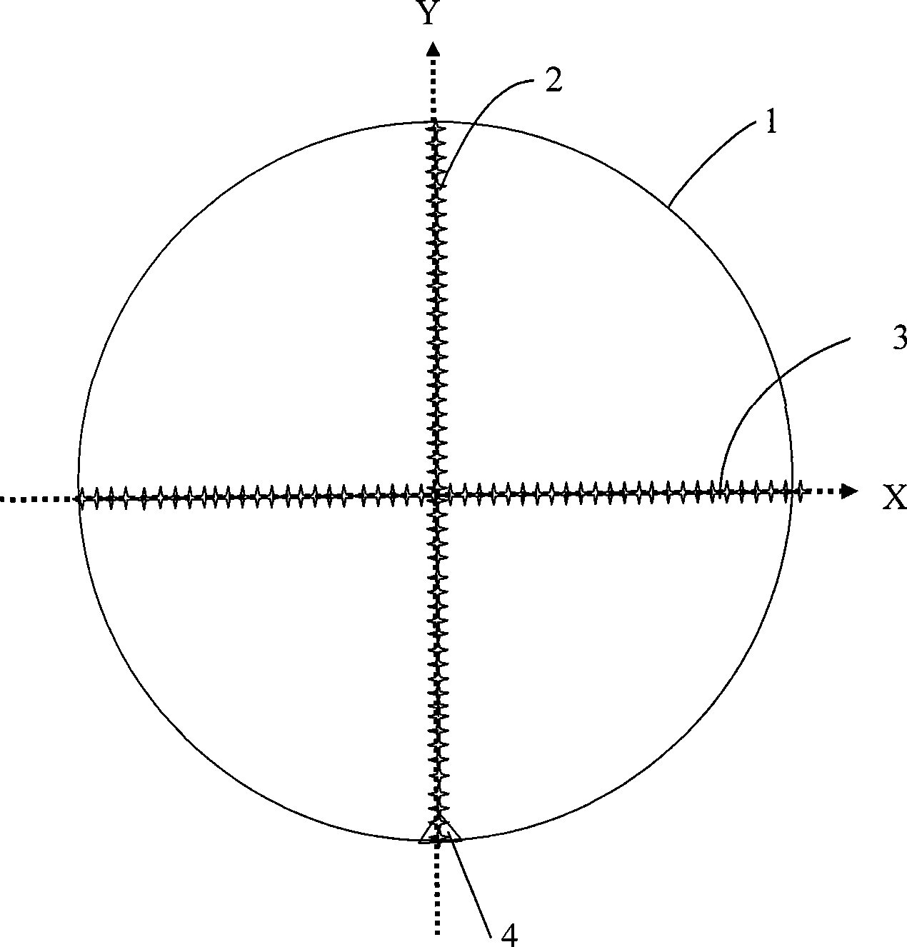
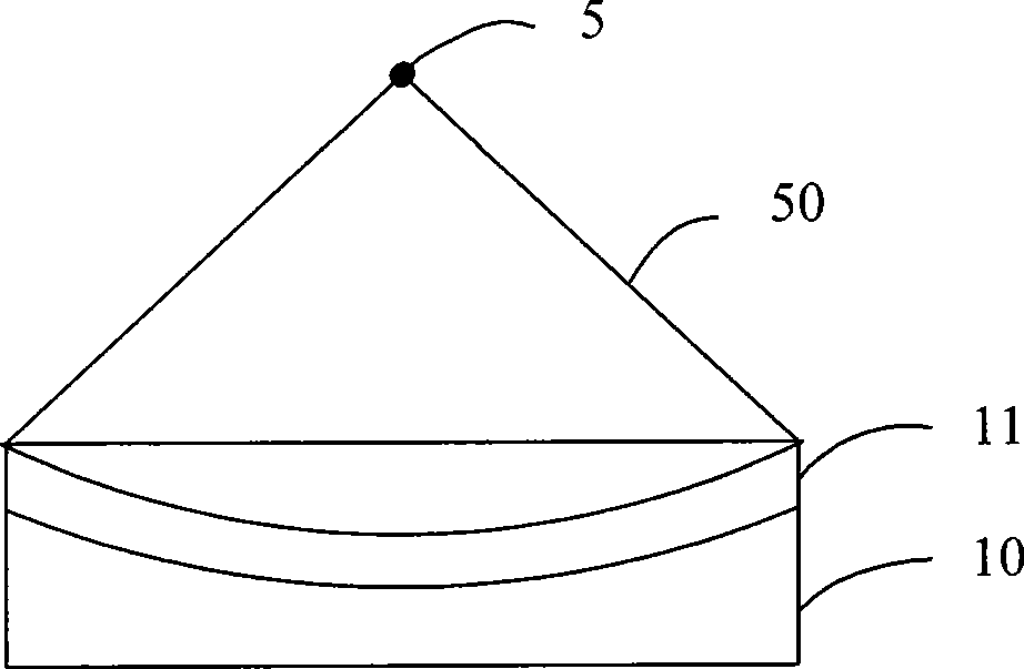
[0012] see figure 2 and image 3 A wafer 1 includes a substrate 10 and an oxide film 11 formed on the substrate in a thermal oxidation step. The detection method of this embodiment is used to detect whether the warpage of the wafer 1 after the thermal oxidation step will affect the subsequent manufacturing process. This detection method comprises the steps:

[0013] The wafer is provided with a mark notch 4, first select two detection lines 2 and 3 crossing the center of the wafer in two...


PUM


Abstract

The invention discloses a method for detecting wafer warp degree, which relates to a detection process in the field of semiconductor. The detecting method comprises the following steps: two detecting lines which are vertical and intersected with a wafer center are selected from the surface of a wafer; and a plurality of detecting points are selected from each detecting line; before the wafer carries out certain processing procedure, the detecting device is used to measure a reference distance; after the wafer carries out certain processing procedure, the detecting device is used to measure the measuring distance; the measuring distance subtracts the corresponding reference distance to obtain a difference value of each measuring point; if the difference value is within the permissible value range, the difference values obtained respectively by two detecting points on the two detecting lines on the same circumference of the wafer are compared; if two difference values are same, the warp of the wafer is proved not to influence the subsequent processing procedure; and if the two difference values are different, the warp of the wafer is proved to influence the subsequent processing procedure. The detecting method provided by the method can effectively and timely detect whether the wafer warp is even or not, and avoid abnormal aligned mark position in the subsequent processing procedure.

Description

technical field [0001] The invention relates to a detection process in the field of semiconductors, in particular to a method for detecting whether the degree of warpage of a wafer will affect subsequent manufacturing processes. Background technique [0002] During the lightly doped source-drain (LDD) photolithography process of the wafer, the position of the alignment mark in some regions of the wafer is often abnormal. This is because after the wafer undergoes certain processes such as thermal oxidation, the wafer warps and exceeds the allowable value range, but no timely compensation and correction is performed. In order to avoid the above situation, the usual practice in the industry is to check whether the degree of warpage of the wafer is within the allowable range after the wafer undergoes certain processes. [0003] In order to facilitate detection, a notch mark 4’ is set at a certain position of the wafer, please refer to figure 1 . The existing detection method ...

Claims


Application Information

Patent Timeline
Patent Type & Authority Applications(China)
IPC IPC(8): H01L21/66G01B11/16
Inventor 刘明源何永根
Owner SEMICON MFG INT (SHANGHAI) CORP
Why Eureka
Try Eureka