Method for programming non-volatile memory with reduced program disturb using modified pass voltages

一种非易失性存储、非易失性的技术,应用在静态存储器、只读存储器、数字存储器信息等方向

Active Publication Date: 2009-02-04
SANDISK TECH LLC
View PDF11 Cites 9 Cited by
  • Summary
  • Abstract
  • Description
  • Claims
  • Application Information

AI Technical Summary

Problems solved by technology

Additionally, band-to-band tunneling or breakdown related to gate-induced drain leakage (GIDL) can occur near the drain of the grounded word line

Method used


Image

  • Method for programming non-volatile memory with reduced program disturb using modified pass voltages
  • Method for programming non-volatile memory with reduced program disturb using modified pass voltages
  • Method for programming non-volatile memory with reduced program disturb using modified pass voltages

Examples


Embodiment Construction

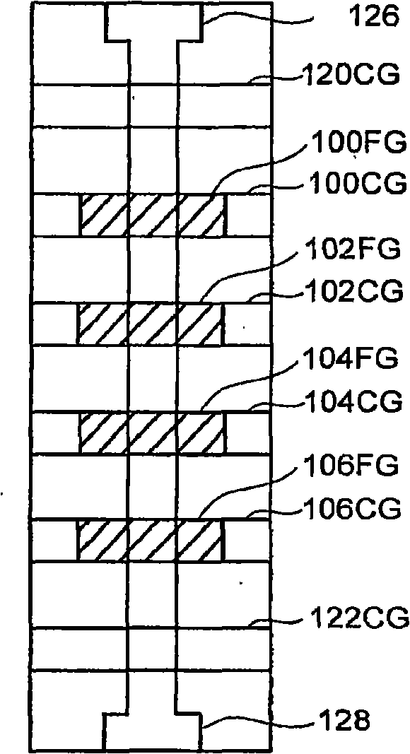
[0027] One example of a non-volatile memory system suitable for implementing the present invention uses a NAND flash memory structure in which multiple transistors are arranged in series between two select gates in a NAND string. figure 1 is a top view showing a NAND string. figure 2 is its equivalent circuit. figure 1 and 2 The NAND string described in includes four transistors 100 , 102 , 104 and 106 arranged in series and sandwiched between a first select gate 120 and a second select gate 122 . Select gates 120 and 122 connect the NAND strings to bit line contacts 126 and source line contacts 128, respectively. Select gates 120 and 122 are controlled by applying appropriate voltages to control gates 120CG and 122CG, respectively. Each of transistors 100, 102, 104, and 106 has a control gate and a floating gate. The transistor 100 has a control gate 100CG and a floating gate 100FG. Transistor 102 includes a control gate 102CG and a floating gate 102FG. Transistor 104 ...


PUM


Abstract

Non-volatile storage elements (1110...1155) are programmed in a manner that reduces program disturb by using modified pass voltages (Vpassl, Vpass2). In particular, during the programming of a selected storage element associated with a selected word line, a higher pass voltage (Vpassl) is applied to word lines associated with previously programmed non-volatile storage elements in the set than to word lines associated with unprogrammed and / or partly programmed non- volatile storage elements in the set. (Vpass2) The pass voltage is sufficiently high to balance the channel potentials on the source and drain sides of the selected word line and / or to reduce leakage of charge between the boosted channel regions.; Optionally, an isolation region is formed between the boosted channel regions by applying a reduced voltage on one or more word lines between the selected word line and the word lines that receive the higher pass voltage.

Description

technical field [0001] The present invention relates to programming non-volatile memory with reduced program disturbance. Background technique [0002] Semiconductor memory has become more and more commonly used in various electronic devices. For example, non-volatile semiconductor memory is used in cellular telephones, digital cameras, personal digital assistants, mobile computing devices, non-mobile computing devices, and other devices. Electrically Erasable Programmable Read Only Memory (EEPROM) and flash memory are among the most common non-volatile semiconductor memories. In contrast to traditional, fully-featured EEPROMs, with flash memory (also a type of EEPROM), the contents of the entire memory array or a portion of the memory can be erased in one step. [0003] Both conventional EEPROM and flash memory use a floating gate positioned above and insulated from a channel region in a semiconductor substrate. The floating gate is positioned between a source region and...

Claims


Application Information

Patent Timeline
Patent Type & Authority Applications(China)
IPC IPC(8): G11C16/04G11C11/56G11C11/34
CPCG11C11/5628G11C16/3418G11C16/0483G11C16/3459G11C16/3427G11C2211/5621G11C16/12
Inventor 格里特·简·赫民克大和田健
Owner SANDISK TECH LLC
Why Eureka
Try Eureka