MEMS switch contact system

A switch and contact technology, applied in the field of MEMS switches, can solve the problems of reducing switch life, reducing conductivity, reducing effectiveness, etc.

Inactive Publication Date: 2008-12-10
ANALOG DEVICES INC
View PDF0 Cites 1 Cited by
  • Summary
  • Abstract
  • Description
  • Claims
  • Application Information

AI Technical Summary

Problems solved by technology

Therefore, the surface contamination layer of the insulation, in addition to reducing the effectiveness, also reduces the conductivity, which reduces the lifetime of the switch

Method used


Image

  • MEMS switch contact system
  • MEMS switch contact system
  • MEMS switch contact system

Examples


Embodiment Construction

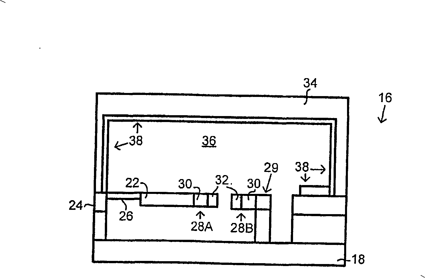
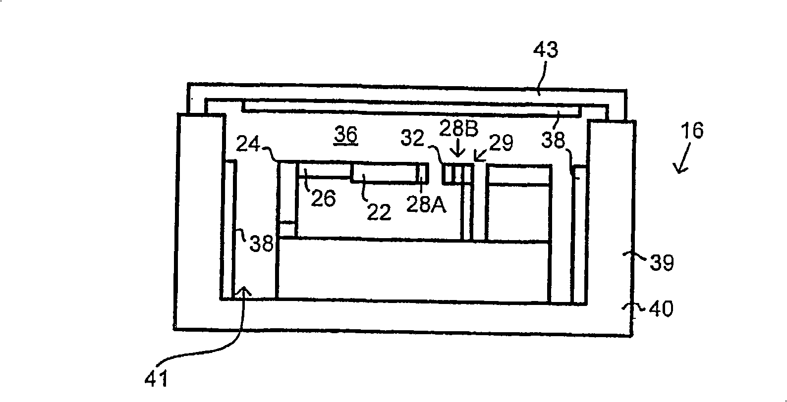
[0016] In an exemplary embodiment, a MEMS switch has contacts formed from a platinum-series-based material. For example, the contact may be formed of ruthenium metal (hereinafter simply referred to as "ruthenium"), ruthenium dioxide, or both. Contacts of this type should have material properties that provide the desired electrical resistance and durability while minimizing undesirable surface contamination layers of the insulation that could degrade switching performance. Details of exemplary embodiments are discussed below.

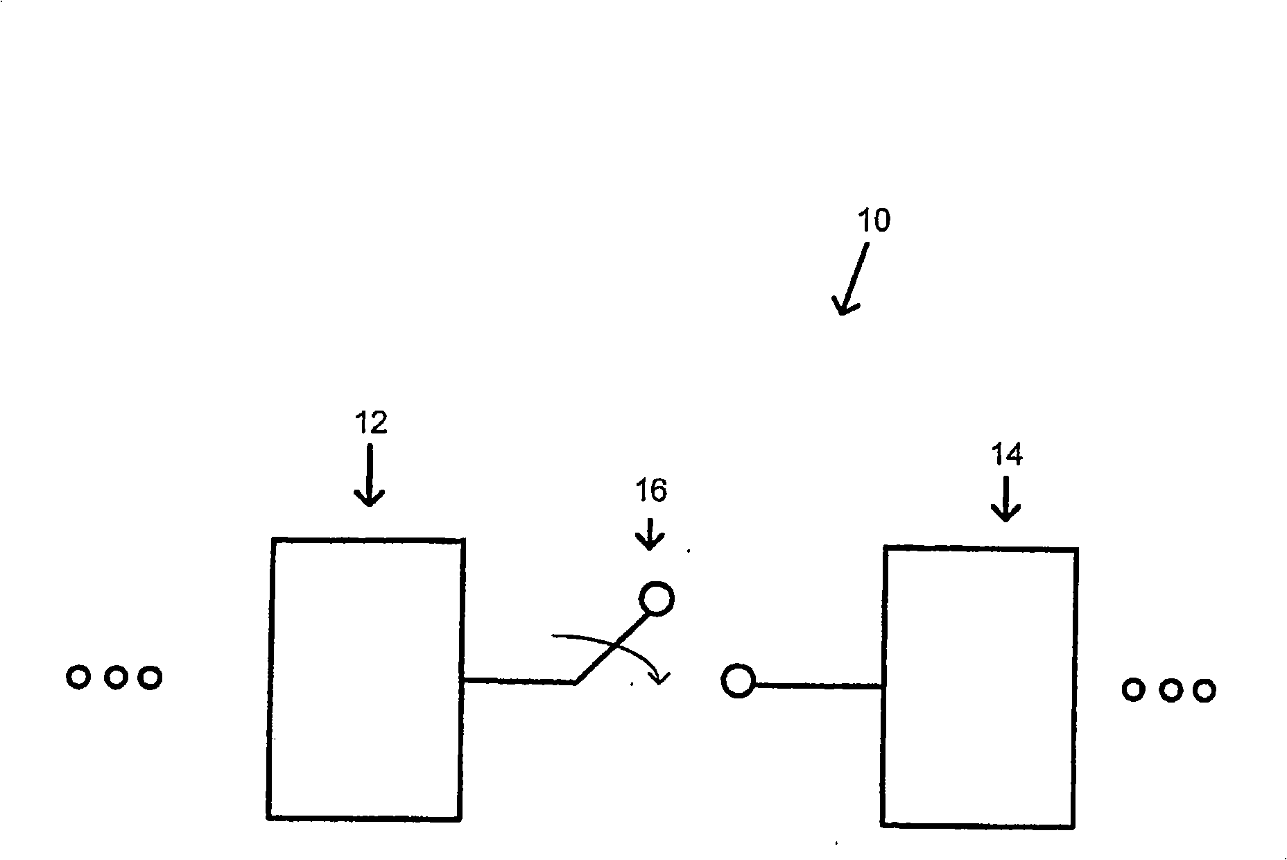
[0017] figure 1 An electronic system 10 is schematically shown utilizing a switch that may be implemented in accordance with an exemplary embodiment of the present invention. Briefly, the electronic system 10 has a first set of components 12 represented by blocks on the left side of the figure, a second set of components 14 represented by blocks on the right side of the figure, and alternately connecting the first and second Switch 16 for group assemb...


PUM


Abstract

A MEMS switch has 1) a first contact, and 2) a second contact that is movable relative to the first contact. At least one of the contacts is electrically conductive and has a platinum-series based material.

Description

technical field [0001] The present invention relates generally to MEMS switches, and more particularly the present invention relates to contact systems for MEMS switches. Background technique [0002] Many types of electrical switches work by moving one member into direct contact with another. For example, a relay switch may have a conductive cantilever that, when actuated, moves to directly contact a stationary conductive element. This direct contact closes the electronic circuit, thereby placing the arm in electrical contact with the fixed element for an ohmic connection. Accordingly, the physical portions of the arms that are in direct contact with each other are known in the art as "ohmic contacts," or simply "contacts," as they are referred to herein. [0003] Contacts are typically made by forming a conductive metal on another surface, which may or may not be an insulator. For example, the cantilever can be formed from silicon and the contacts at the ends of the can...

Claims


Application Information

Patent Timeline
Patent Type & Authority Applications(China)
IPC IPC(8): H01H1/00
CPCH01H1/0036H01H1/0237H01H59/0009H01H2001/0052
Inventor 马克·席尔默约翰·狄克逊
Owner ANALOG DEVICES INC
Why Eureka
Try Eureka