Optical recording medium
An optical recording medium and recording layer technology, which can be applied to optical recording carriers, optical recording systems, recording/reproducing by optical methods, etc., and can solve the problem of high manufacturing cost of optical recording media
- Summary
- Abstract
- Description
- Claims
- Application Information
AI Technical Summary
Problems solved by technology
Method used
Image
Examples
Embodiment 1 to 5
[0069] -Preparation of Optical Recording Medium-
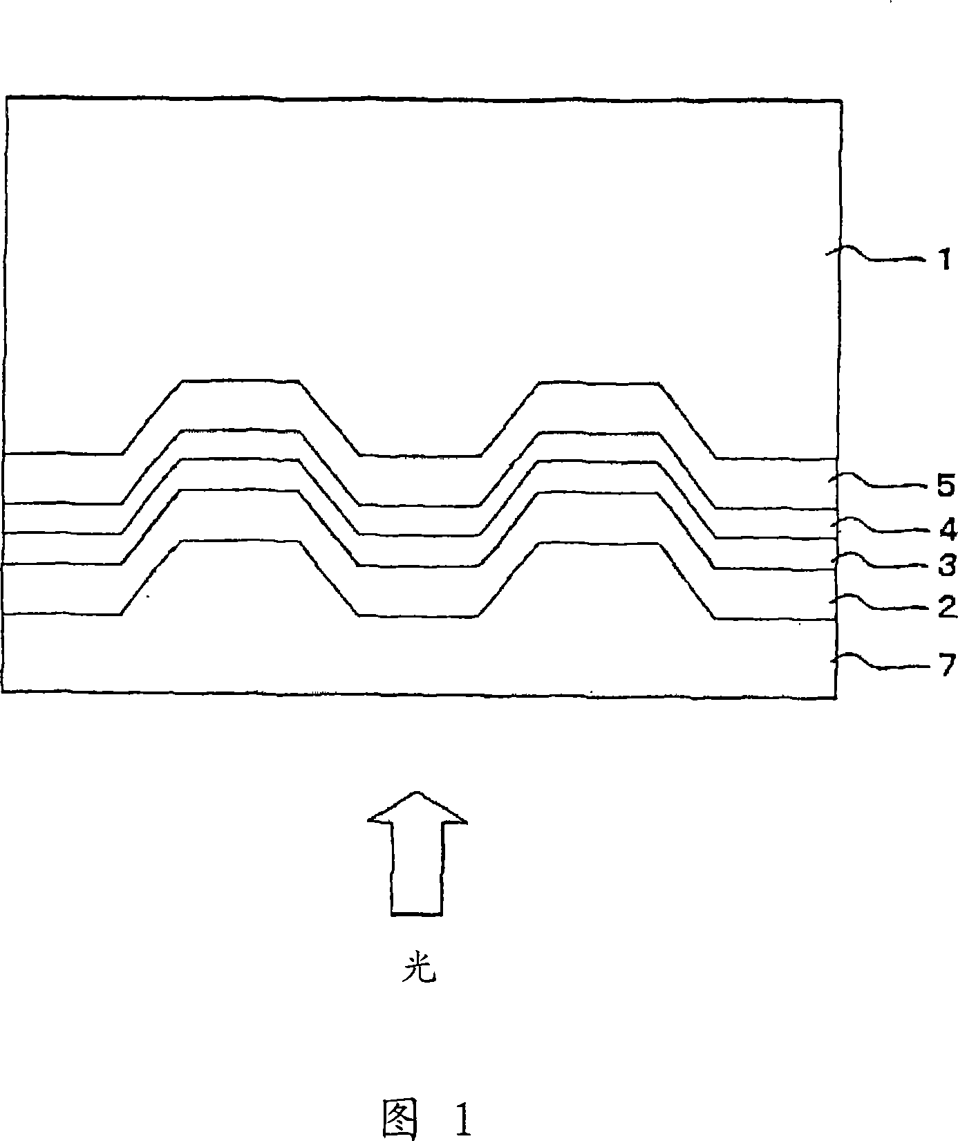
[0070] A substrate made of polycarbonate resin having a diameter of 12 cm and a thickness of 1.1 mm on which grooves were formed was used. The pitch between the grooves was 0.32 μm, the width of the pitch where information was recorded was 0.165 μm, and the depth of the grooves was 22 nm.
[0071] Films were sequentially formed on the substrate using a magnetron sputtering apparatus DVD-Sprinter manufactured by Unaxis.
[0072] First, a 140 nm-thick reflective layer was formed using an Ag-Bi target (Bi content: 0.5 atomic %).
[0073] Next, use Nb 2 o 5 : SiO 2 =85:15 (mol %) targets to form the second dielectric layer with 5 different thicknesses shown in Table 1 on the reflective layer.
[0074] Then use the composition with Ge 9.5 Sb 66 sn 18 mn 6.5 (atomic %) target, a recording layer with a thickness of 14 nm was formed on the second dielectric layer with 5 different thicknesses.
[0075] Next, using ZnS:SiO 2 ...
Embodiment 6
[0088] -Preparation of Optical Recording Medium-
[0089] A substrate made of polycarbonate resin having a diameter of 12 cm and a thickness of 1.1 mm on which grooves were formed was used. The pitch between the grooves was 0.32 μm, the width of the pitch where information was recorded was 0.165 μm, and the depth of the grooves was 22 nm.
[0090] Films were sequentially formed on the substrate using a magnetron sputtering apparatus DVD-Sprinter manufactured by Unaxis.
[0091] First, a 140 nm-thick reflective layer was formed using an Ag-Bi target (Bi content: 0.5 atomic %).
[0092] Next, use Nb 2 o 5 : SiO 2 =85:15 (mol%) target, a second dielectric layer with a thickness of 8 nm was formed on the reflective layer.
[0093] Then use the composition with Ge 5.5 Sb 66 sn 18 mn 6.5 Ga 4 (atomic %) target, a recording layer with a thickness of 14 nm was formed on the second dielectric layer.
[0094] Next, using ZnS:SiO 2 =70:30 (mol%) target, the first dielectric l...
Embodiment 7 to 28
[0103] A substrate made of polycarbonate resin having a diameter of 12 cm and a thickness of 1.1 mm on which grooves were formed was used. The pitch between the grooves was 0.32 μm, the width of the pitch where information was recorded was 0.165 μm, and the depth of the grooves was 22 nm.
[0104] Films were sequentially formed on the substrate using a magnetron sputtering device DVD-Sprinter from Unaxis.
[0105] First, a 140 nm-thick reflective layer was formed using an Ag-Bi target (Bi content: 0.5 atomic %).
[0106] Next, use Nb respectively 2 o 5 ·SiO2 2 、 Ta 2 o 5 ·SiO2 2 and Nb 2 o 5 ·SiO2 2 ·Ta 2 o 5 target, a second dielectric layer with a thickness of 8 nm was formed on the reflective layer.
[0107] Use composition as Ge 5.5 Sb 66 sn 18 mn 6.5 Ga 4 (atomic %) target, a recording layer with a thickness of 14 nm was formed on the second dielectric layer.
[0108] Next, using ZnS:SiO 2 =70:30 (mol%) target, the first dielectric layer was formed on t...
PUM
| Property | Measurement | Unit |
|---|---|---|
| thickness | aaaaa | aaaaa |
| thickness | aaaaa | aaaaa |
| thickness | aaaaa | aaaaa |
Abstract
Description
Claims
Application Information
 - R&D
- Intellectual Property
- Life Sciences
- Materials
- Tech Scout
- Unparalleled Data Quality
- Higher Quality Content
- 60% Fewer Hallucinations
Browse by: Latest US Patents, China's latest patents, Technical Efficacy Thesaurus, Application Domain, Technology Topic, Popular Technical Reports.
© 2025 PatSnap. All rights reserved.Legal|Privacy policy|Modern Slavery Act Transparency Statement|Sitemap|About US| Contact US: help@patsnap.com

