Solid-state image sensor
A technology for solid-state imaging elements and semiconductors, which can be used in electric solid-state devices, electrical components, semiconductor devices, etc., and can solve problems such as superimposed noise.
- Summary
- Abstract
- Description
- Claims
- Application Information
AI Technical Summary
Problems solved by technology
Method used
Image

Examples
no. 1 approach
[0053]
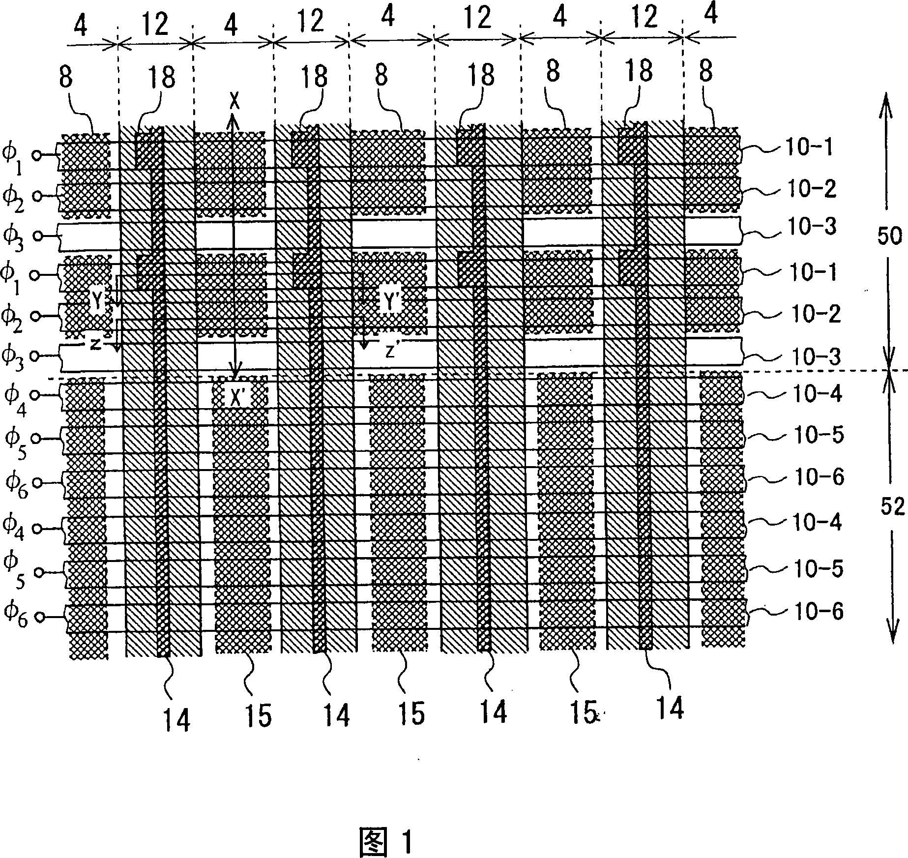
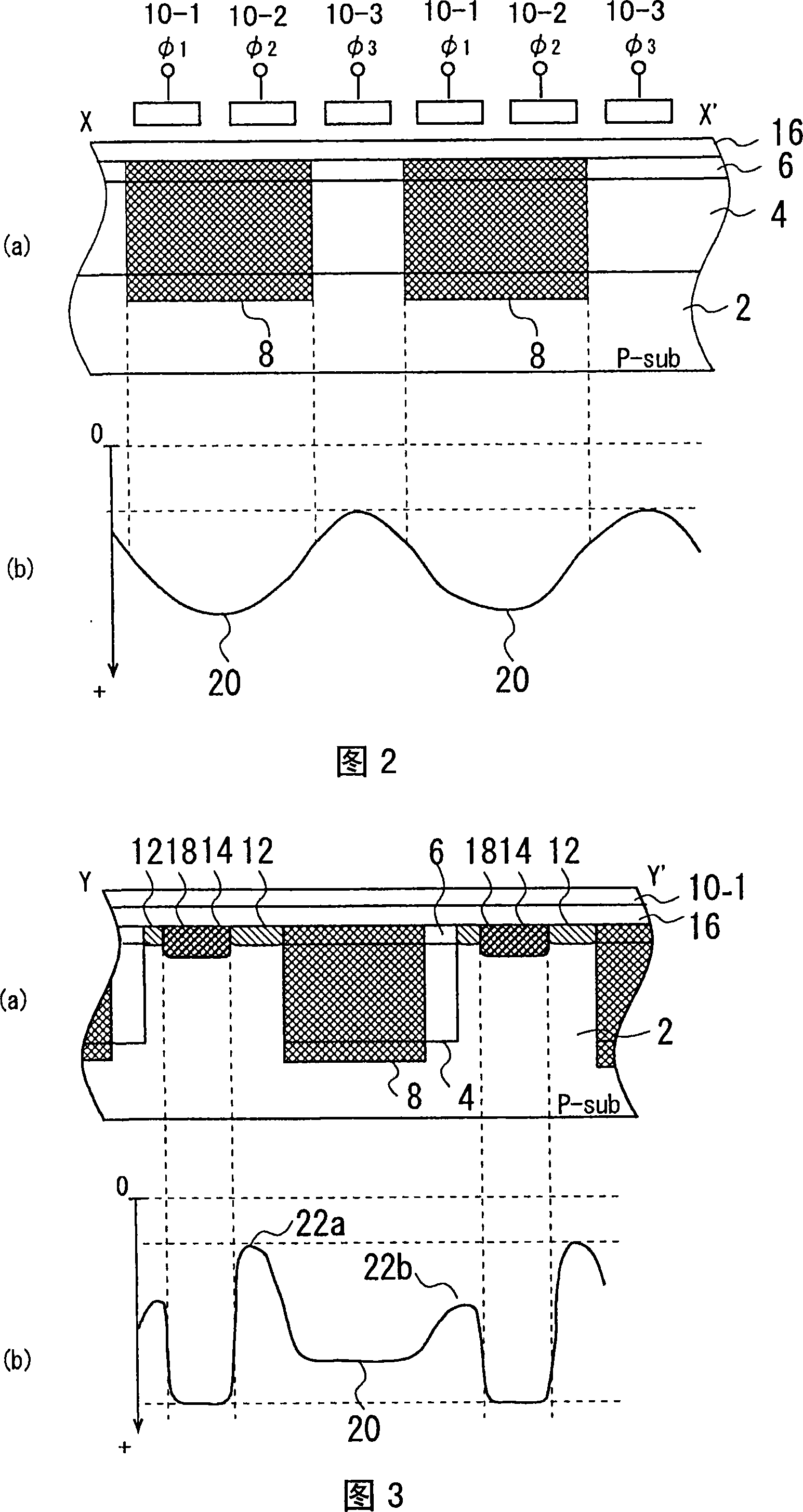
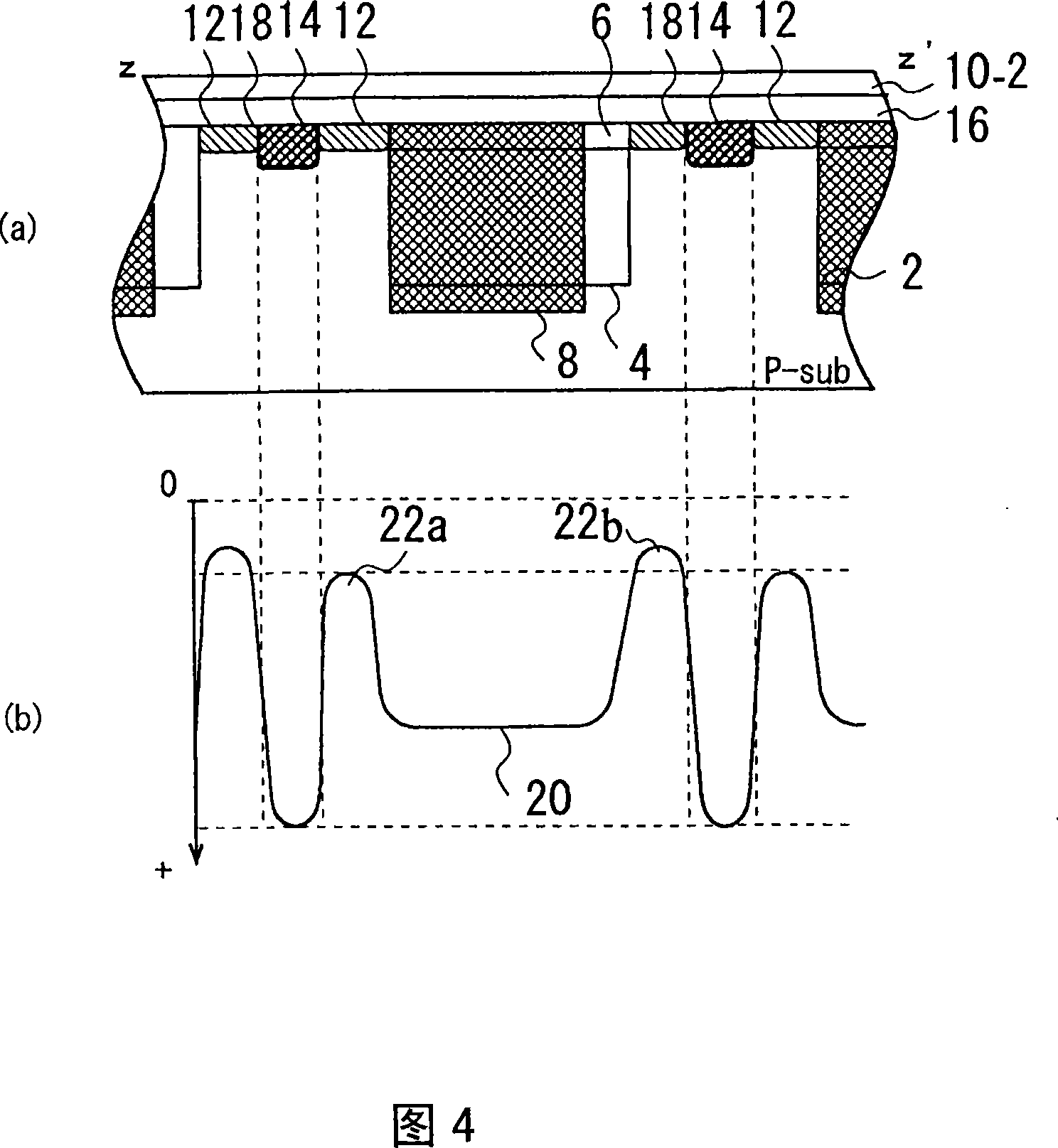
[0054] FIG. 1 is a plan view showing the vicinity of the boundary between the imaging unit 50 and the storage unit 52 of the CCD solid-state imaging device in the first embodiment of the present invention. 2 shows a cross-sectional view and potential distribution of the imaging unit 50 in the X-X' direction, and FIG. 3 shows a cross-sectional view and potential distribution of the imaging unit 50 in the Y-Y' direction.
[0055] First, the planar configuration of the imaging unit 50 of the CCD solid-state imaging device in this embodiment will be described with reference to FIG. 1 . A plurality of first channel regions 4 are provided in parallel to each other in the imaging unit 50 . The first channel region 4 is formed with a predetermined gap, and a plurality of isolation regions 12 are provided in parallel to each other in the gap. The first channel region 4 is electrically divided by two adjacent separation regions 12 . The first channel region 4 partitioned by...
no. 2 approach
[0094] Next, a CCD solid-state imaging device according to another embodiment of the present invention will be described.
[0095] FIG. 11 is a schematic view showing the vicinity of the boundary between the imaging unit 50 and the storage unit 52 of the CCD solid-state imaging device in the second embodiment. Shown in Fig. 11: be arranged on the first channel region 4 that extends parallel to each other on the semiconductor substrate; Be arranged in the gap of the first channel region 4, the second, the third channel region 8,15; ~ the separation region 12 electrically divided by the third channel region 4, 8, 15; the overflow trench region 14 having the protrusion 18; the first transfer electrodes 10-1 to 10-3 and the second transfer electrodes 10-4~ 10-6.
[0096] The overflow trench region 14 of this embodiment is provided in every other isolation region 12 . Furthermore, the overflow trench region 14 extends near the center of the separation region 12 , and unlike the f...
no. 3 approach
[0101] FIG. 12 is a schematic view showing the vicinity of the boundary between the imaging unit 50 and the storage unit 52 of the CCD solid-state imaging device in the third embodiment. Figure 12 shows in the same manner as in Figure 11: a first channel region 4, a second channel region 8, a third channel region 15, a separation region 12, an overflow trench region 14 with a protrusion 18, The first transfer electrodes 10-1 to 10-3 and the second transfer electrodes 10-4 to 10-6.
[0102] The overflow trench regions in this embodiment are provided in all the separation regions 12, and are arranged to extend near the center of the separation regions 12, and each overflow trench region 14 has a direction toward the adjacent two second channel regions 8. The protrusions 18 on both sides. In the discharge drive of the present embodiment, the information charges accumulated in the second channel region 8 are discharged to two adjacent overflow trench regions 14 via the protruding...
PUM
 Abstract
Description
Claims
Application Information
 - R&D
- Intellectual Property
- Life Sciences
- Materials
- Tech Scout
- Unparalleled Data Quality
- Higher Quality Content
- 60% Fewer Hallucinations
Browse by: Latest US Patents, China's latest patents, Technical Efficacy Thesaurus, Application Domain, Technology Topic, Popular Technical Reports.
© 2025 PatSnap. All rights reserved.Legal|Privacy policy|Modern Slavery Act Transparency Statement|Sitemap|About US| Contact US: help@patsnap.com